Pictures of my MA-7 development board
 |
|---|
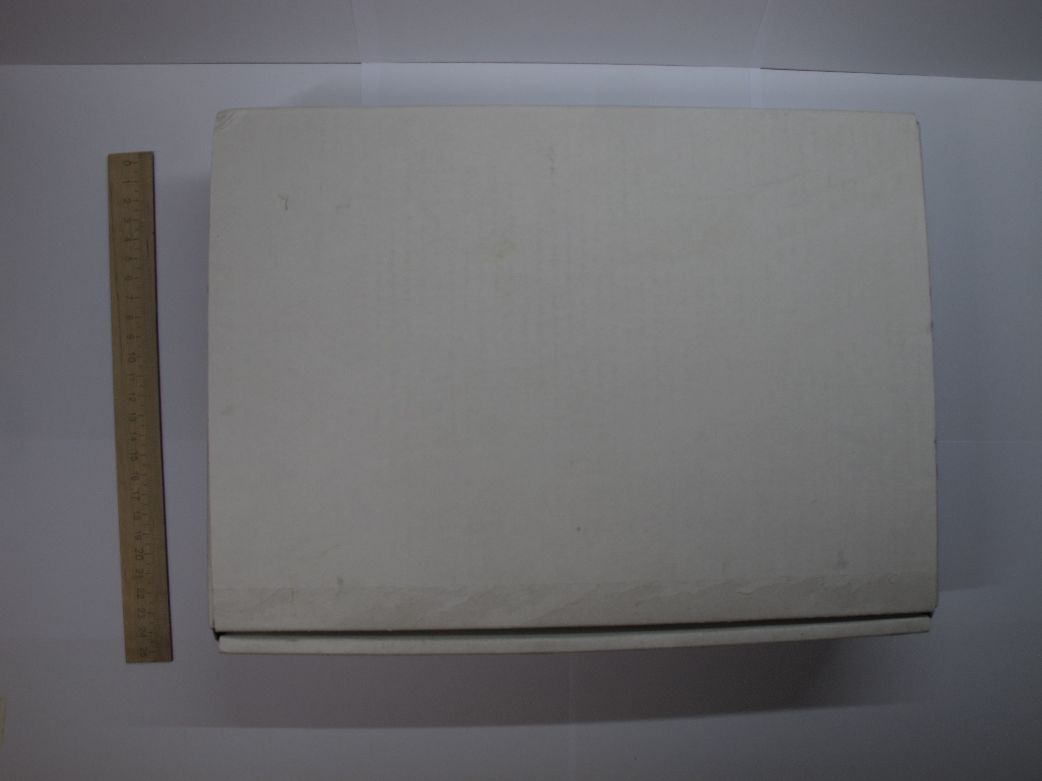
| Box. |
 |
|---|
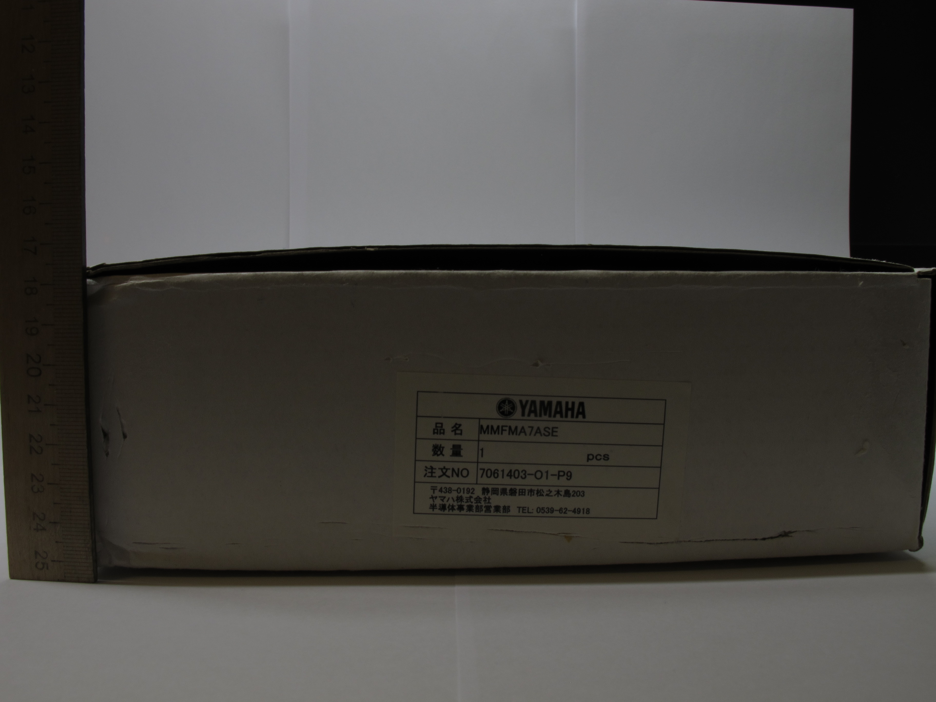
| The only thing written on the box. |
 |
|---|
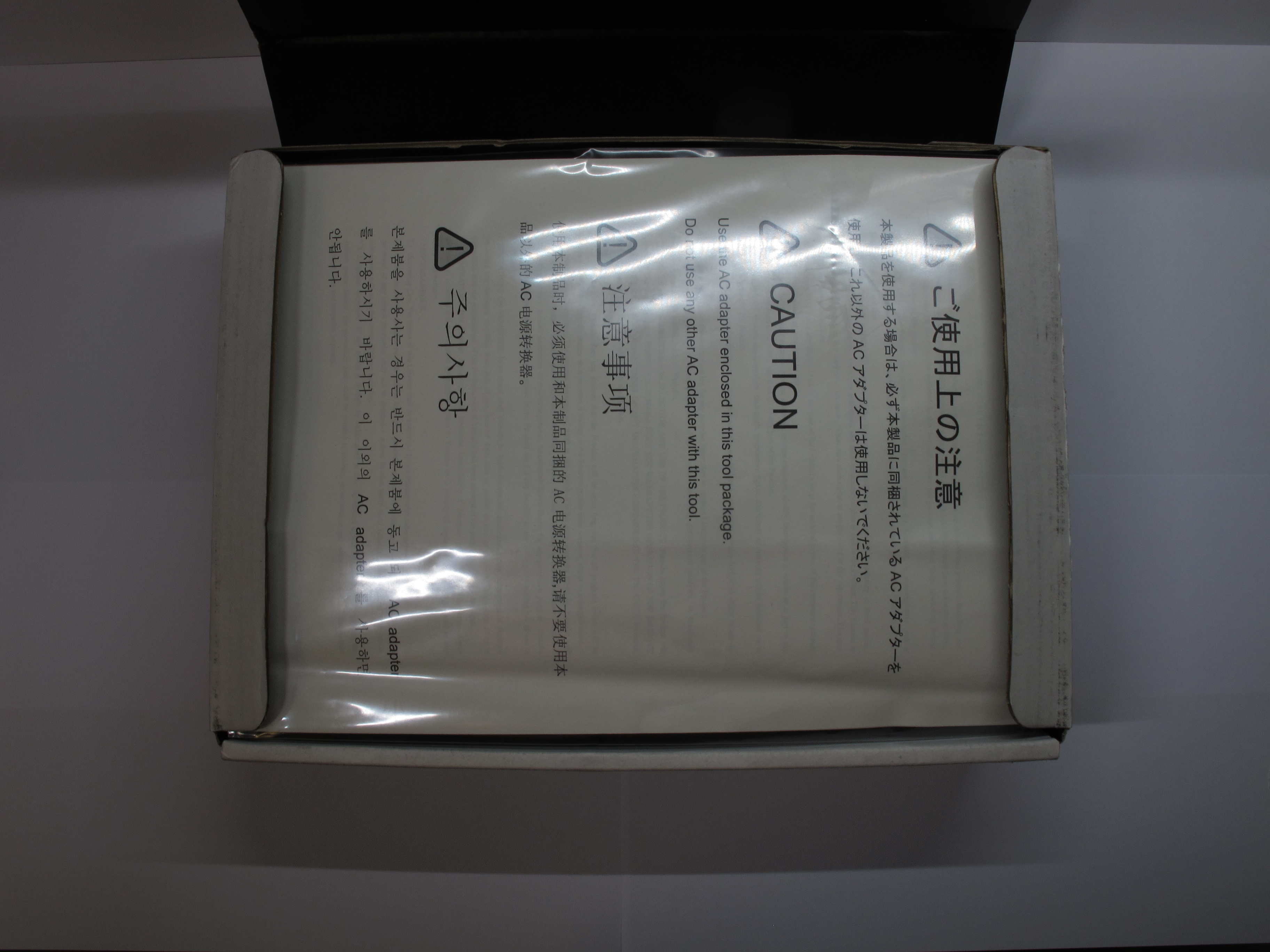
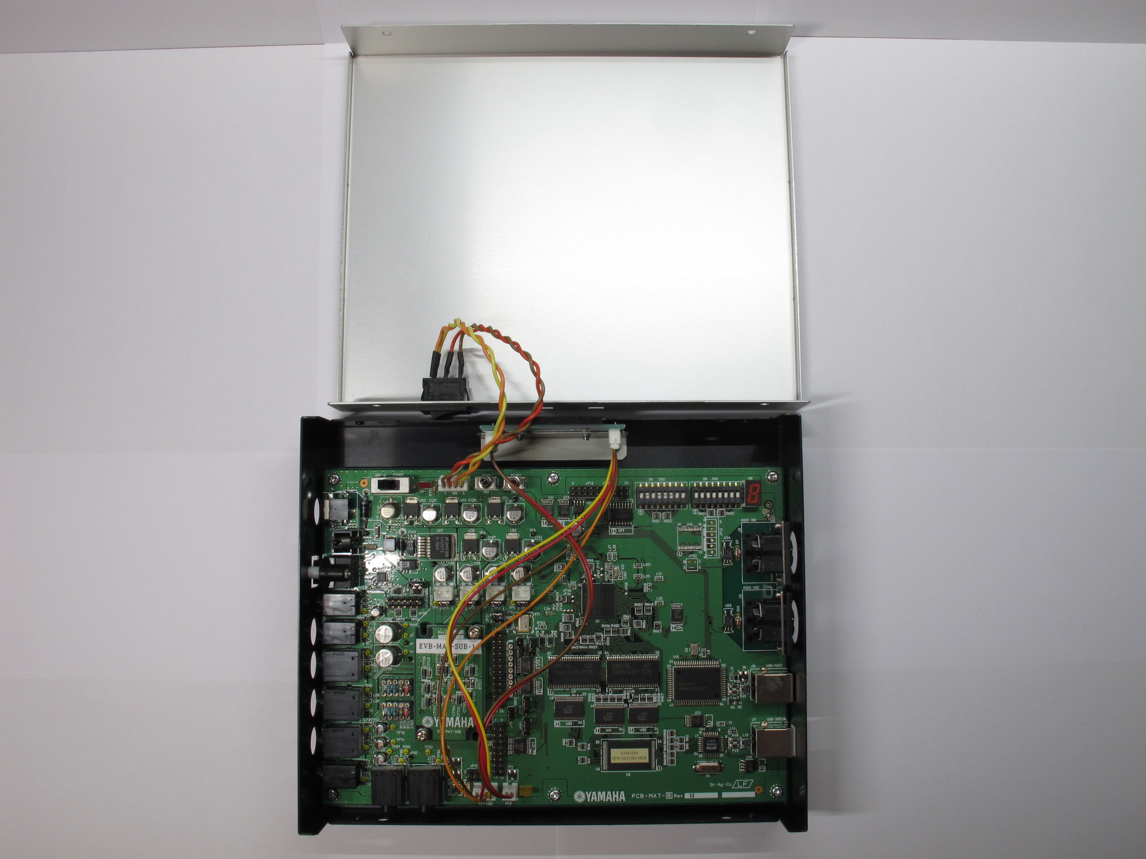
| Inside the box lies the caution blah blah. |
 |
|---|
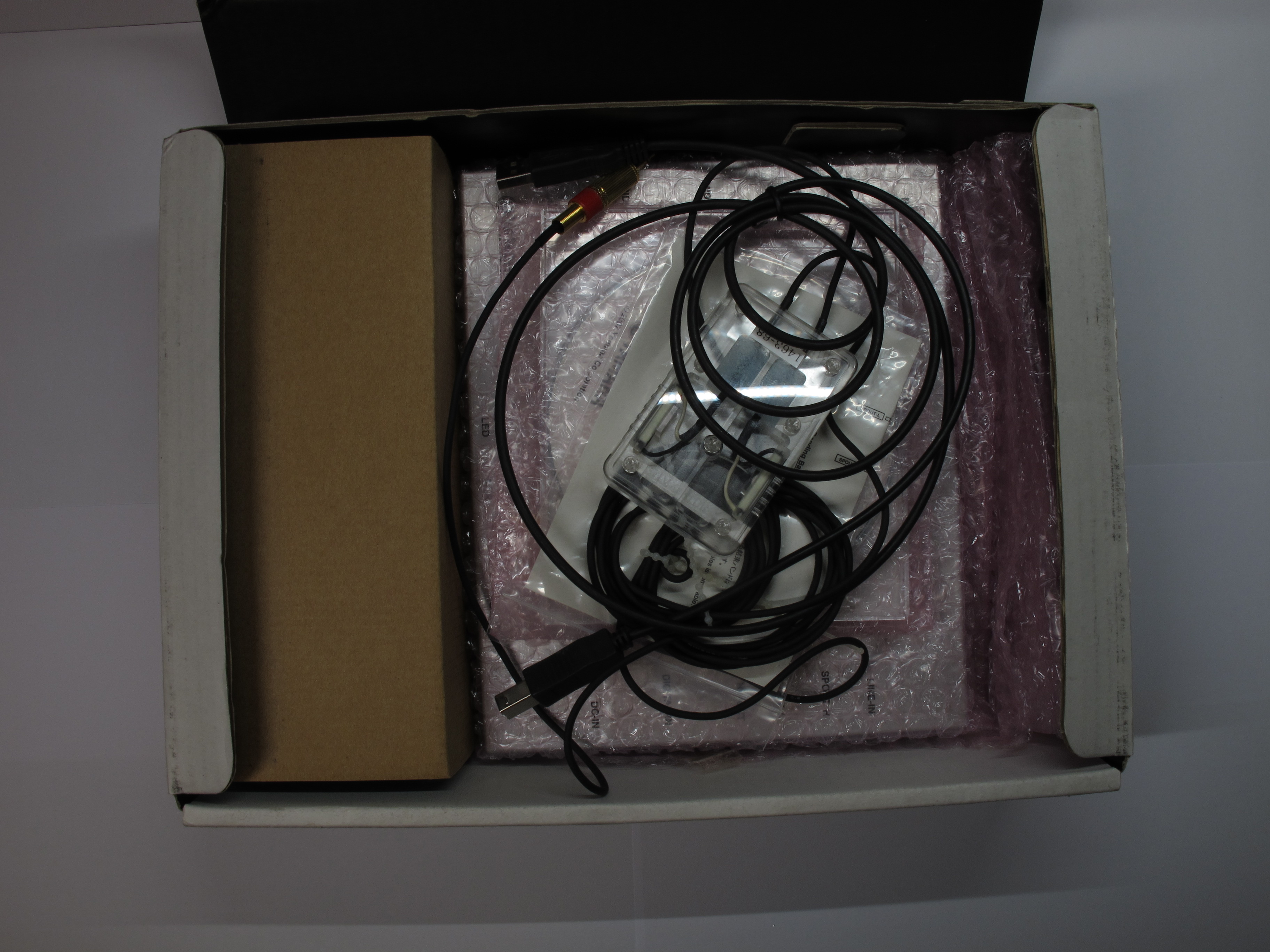
| Under the caution lie the wires. |
 |
|---|
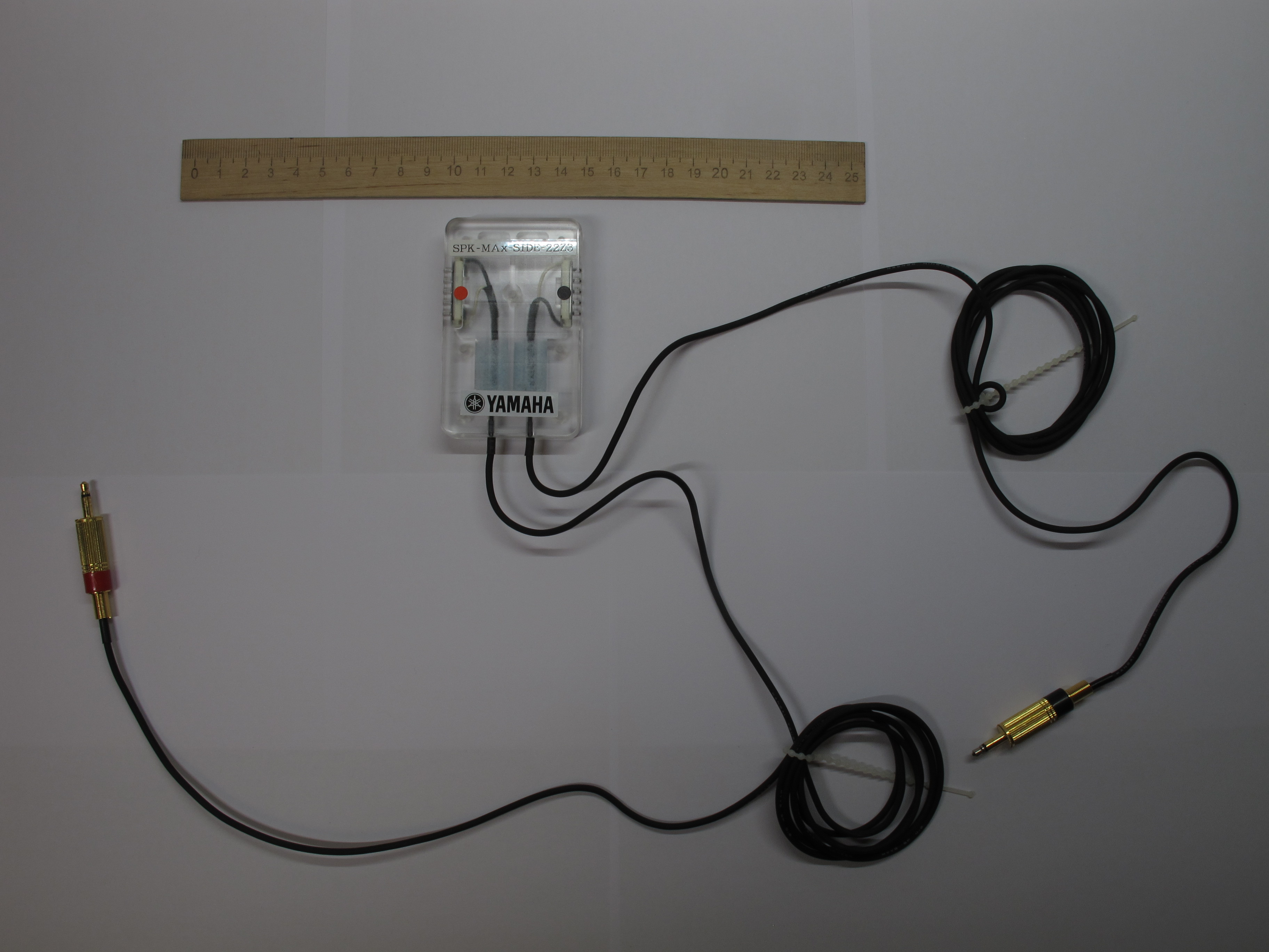
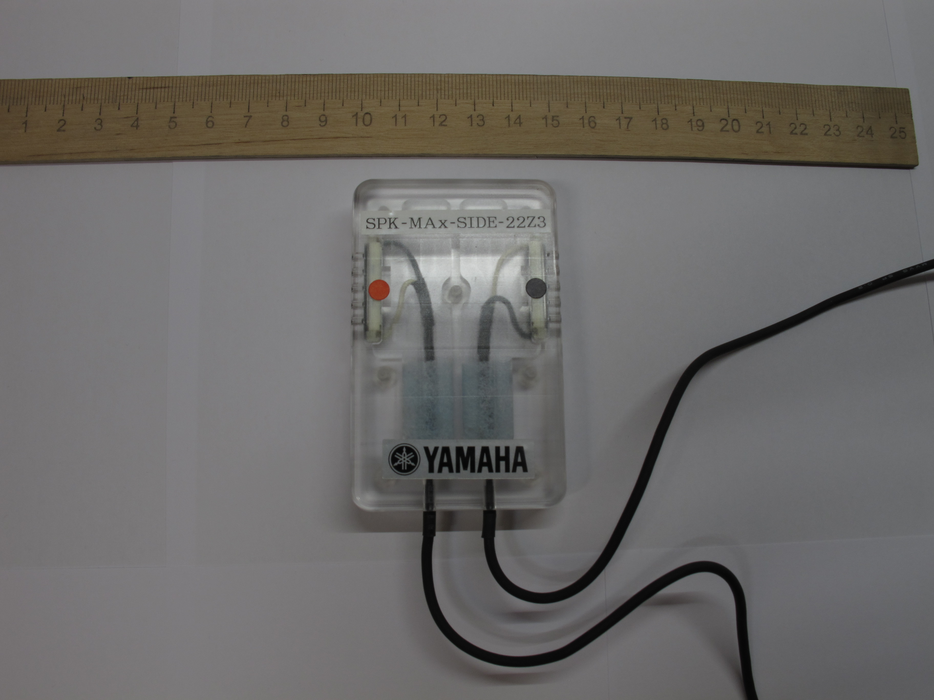
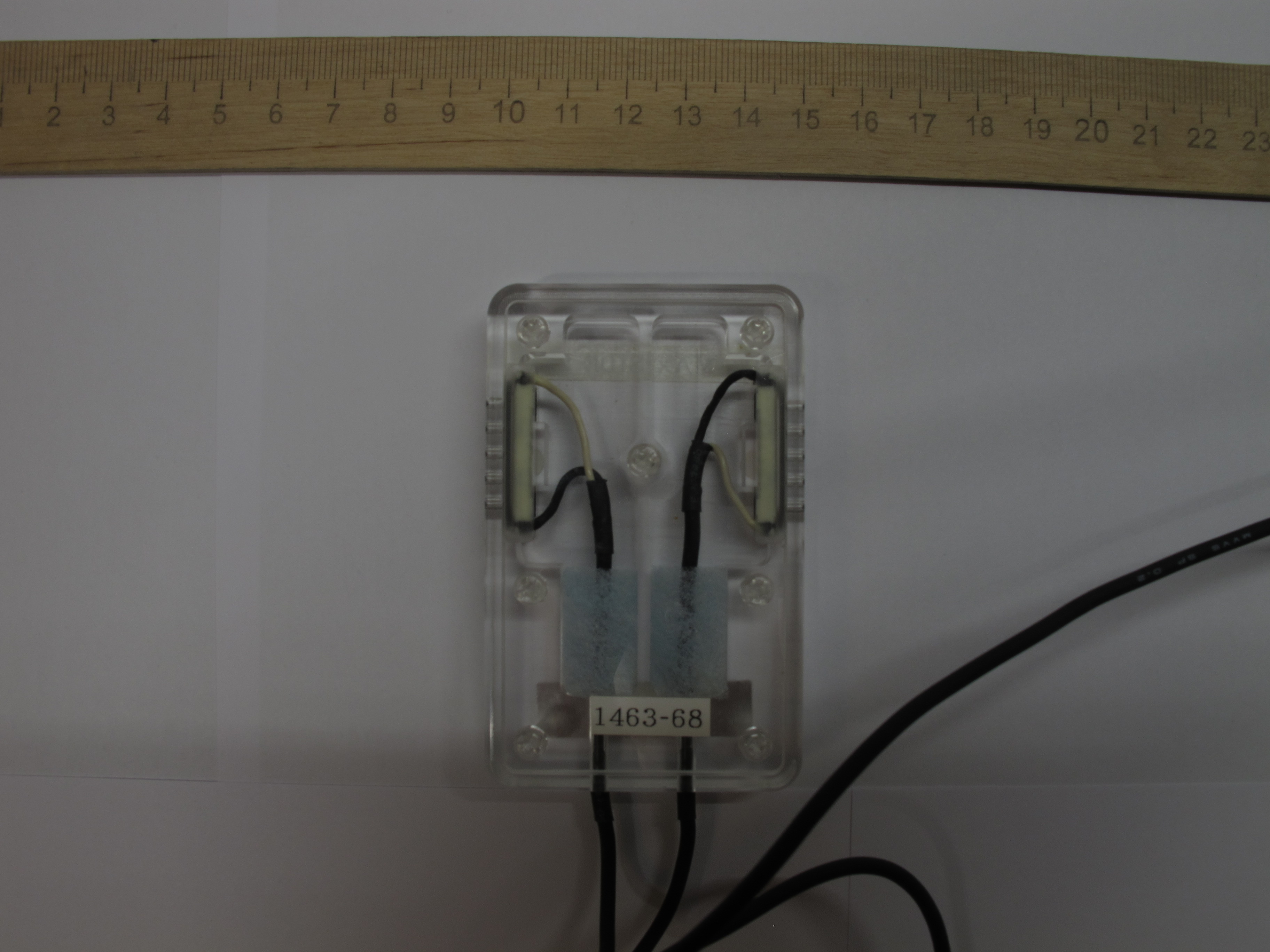
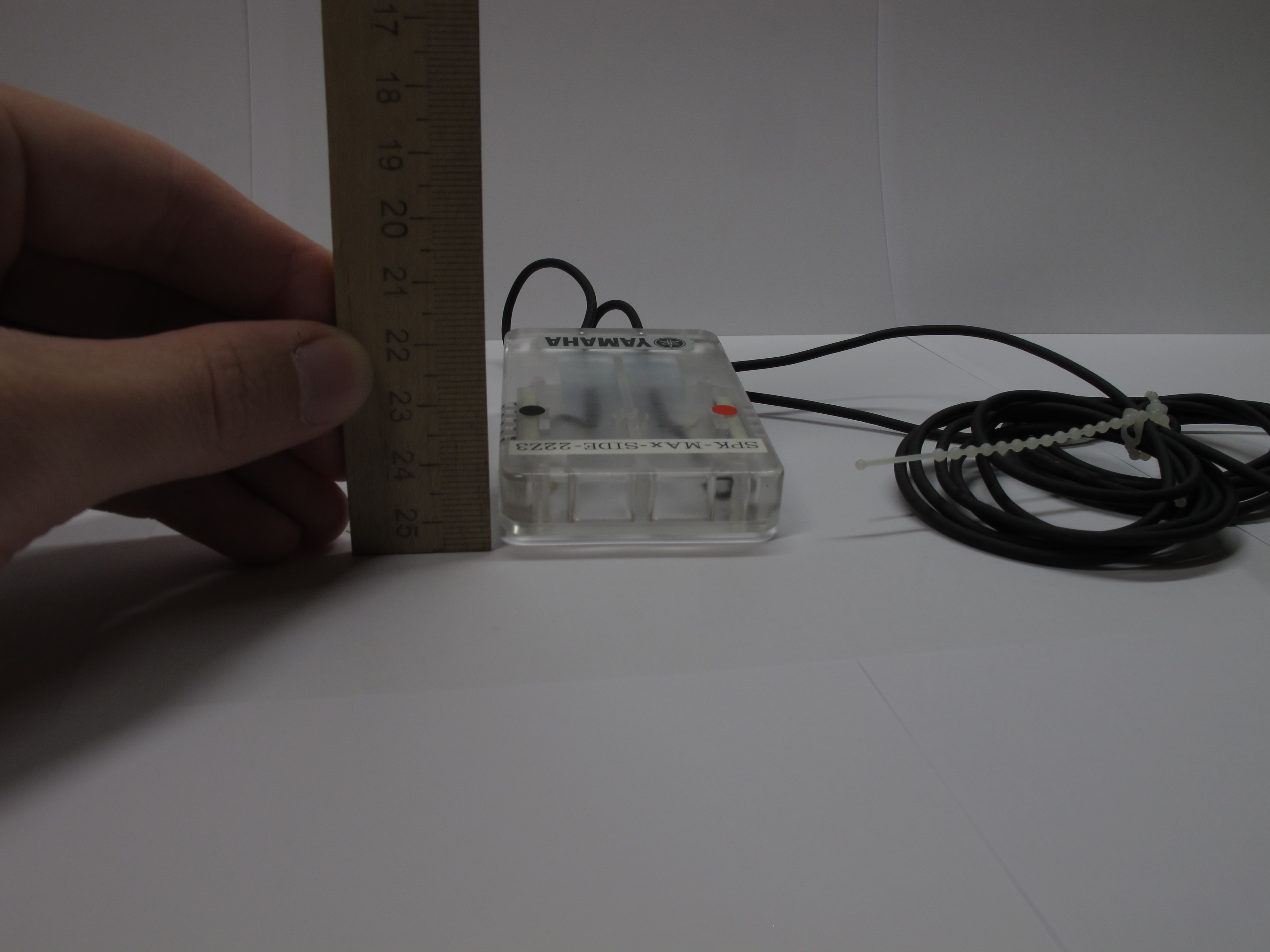
| Mobile phone speakers simulator. |
 |
|---|
| Main simulator. |
 |
|---|
| Simulator's underside. |
 |
|---|
| Simulator's thickness. |
 |
|---|
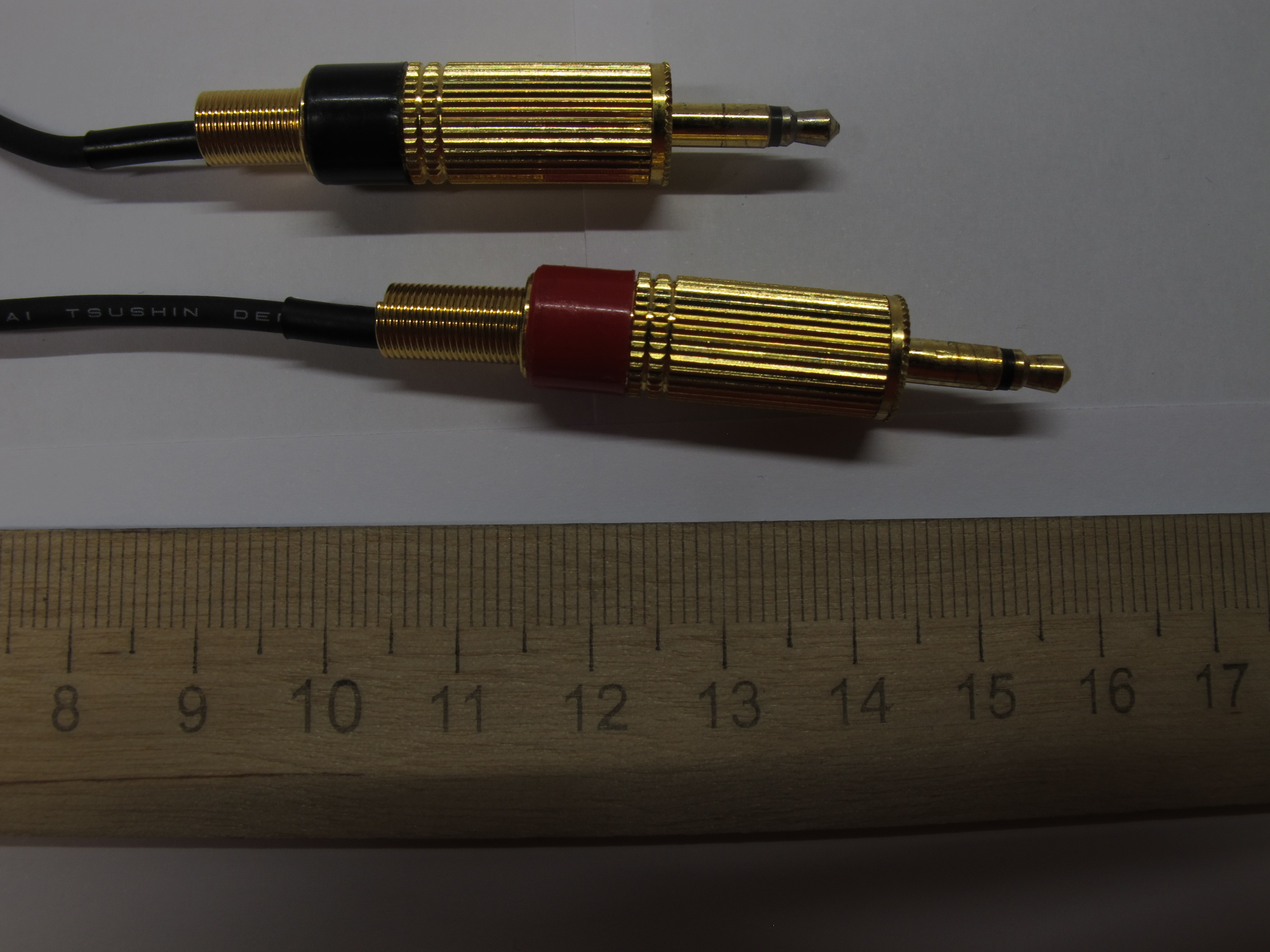
| Simulator's beefy audio jacks, one per channel. |
 |
|---|
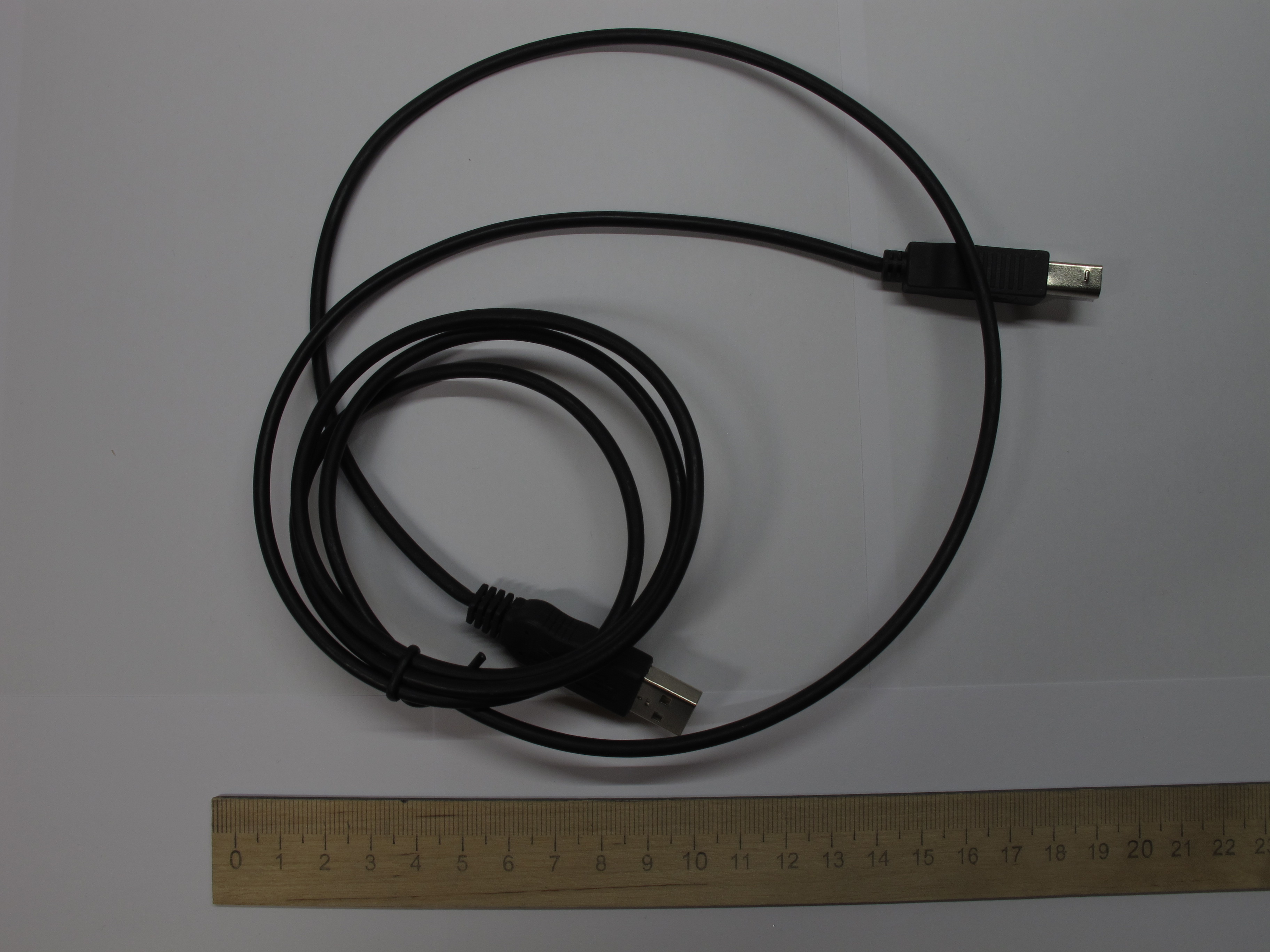
| USB cable, nothing special. |
 |
|---|
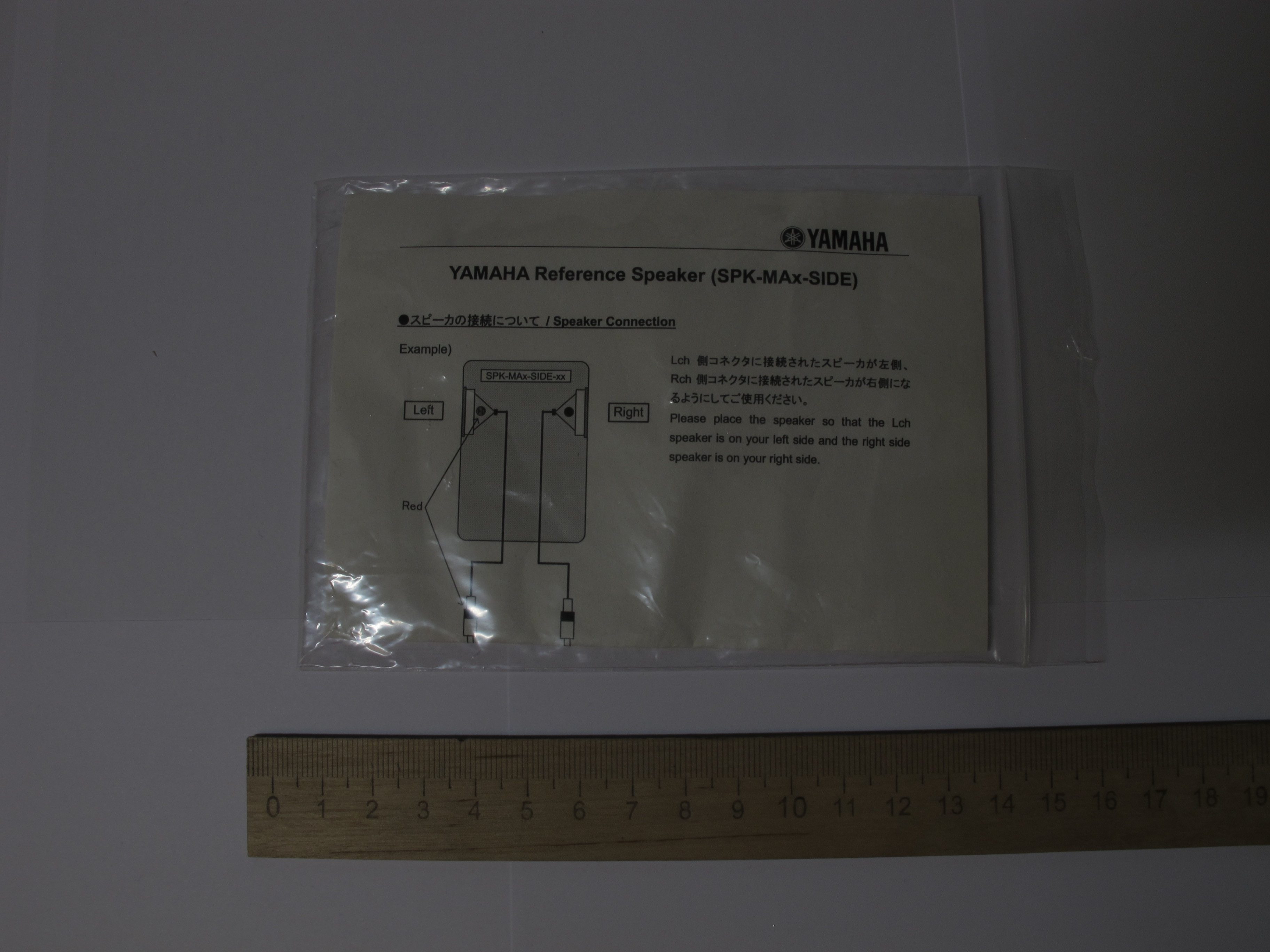
| The package and instruction for phone speaker simulator. |
 |
|---|
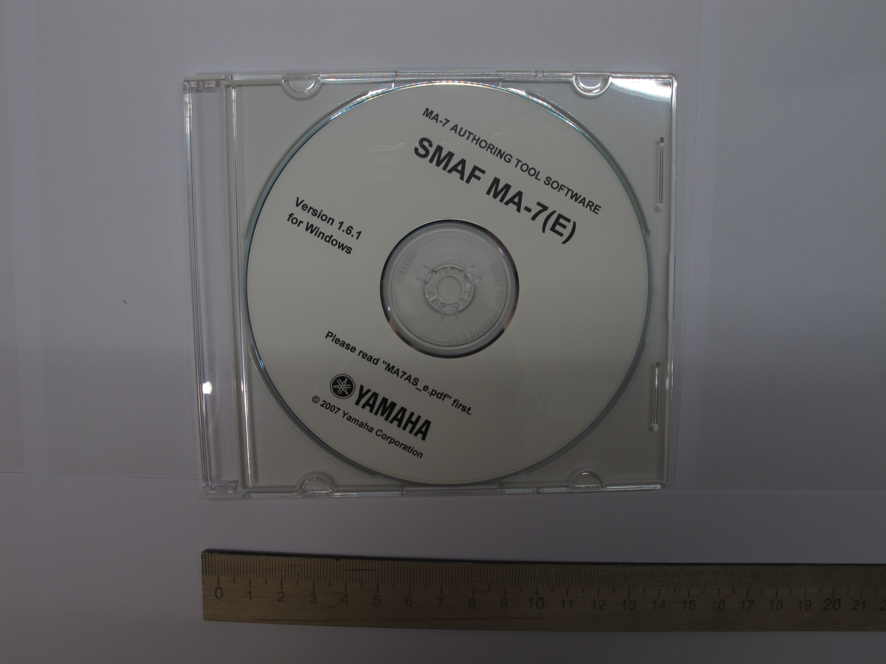
| Firmware and docs disc. |
 |
|---|
| Firmware and docs disc, naked. |
 |
|---|
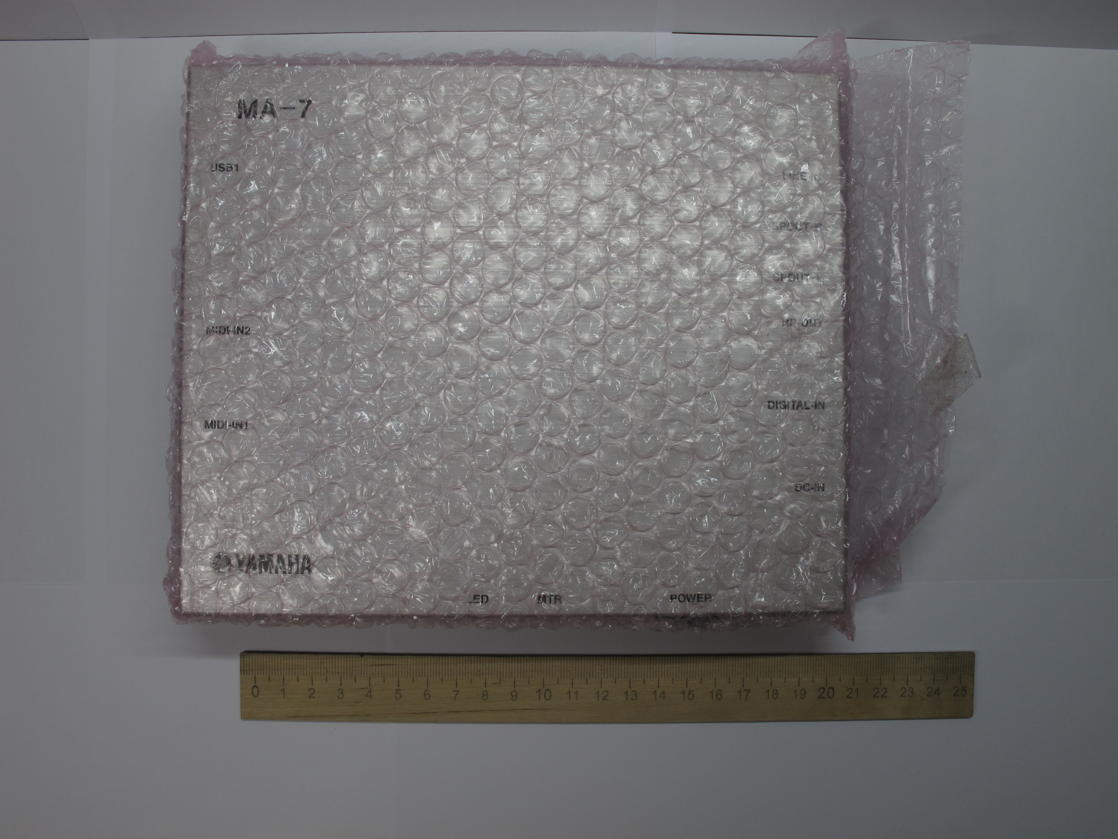
| The dev board itself. |
 |
|---|
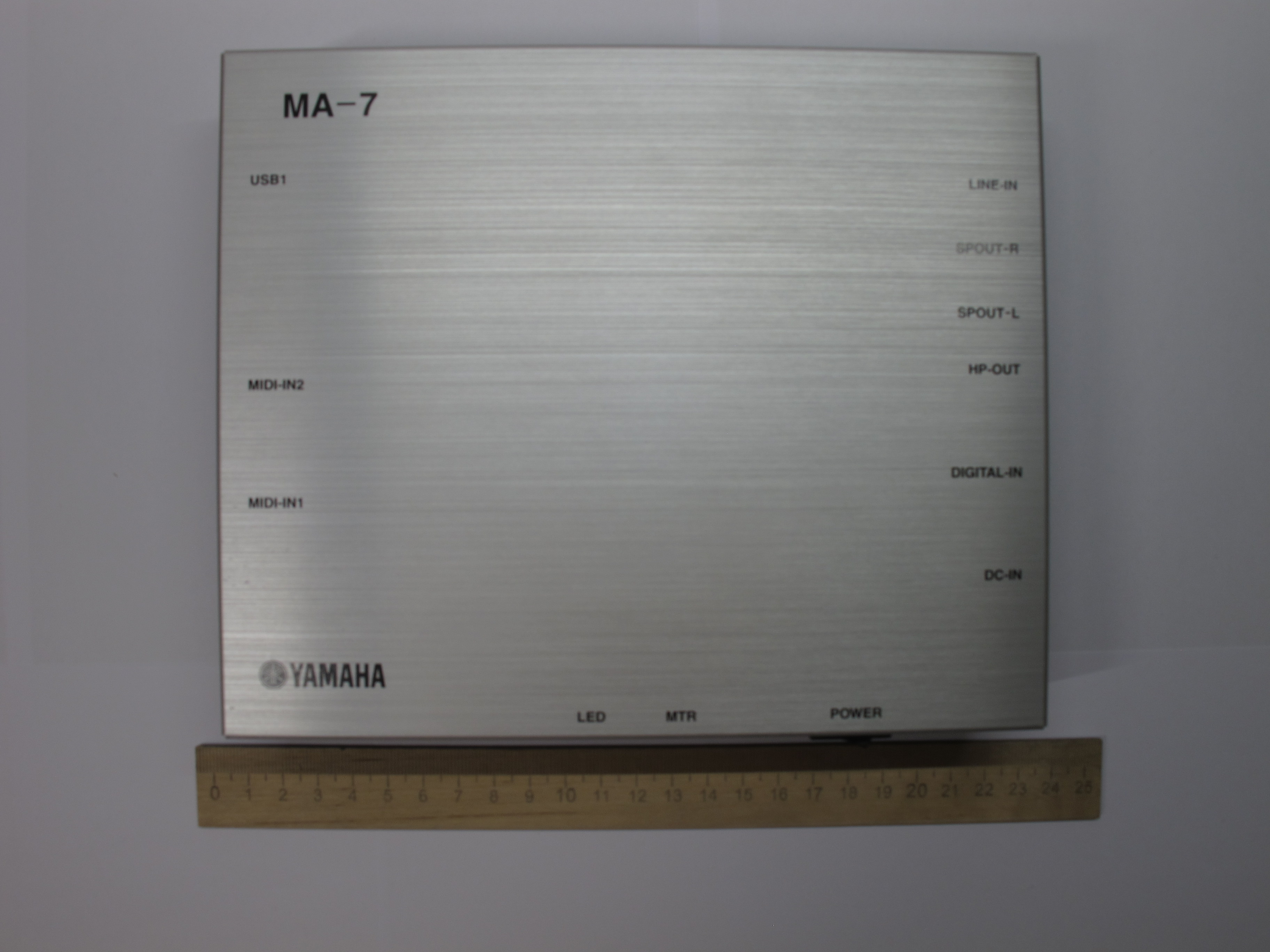
| The dev board itself, naked. |
 |
|---|
| The dev board front panel. |
 |
|---|
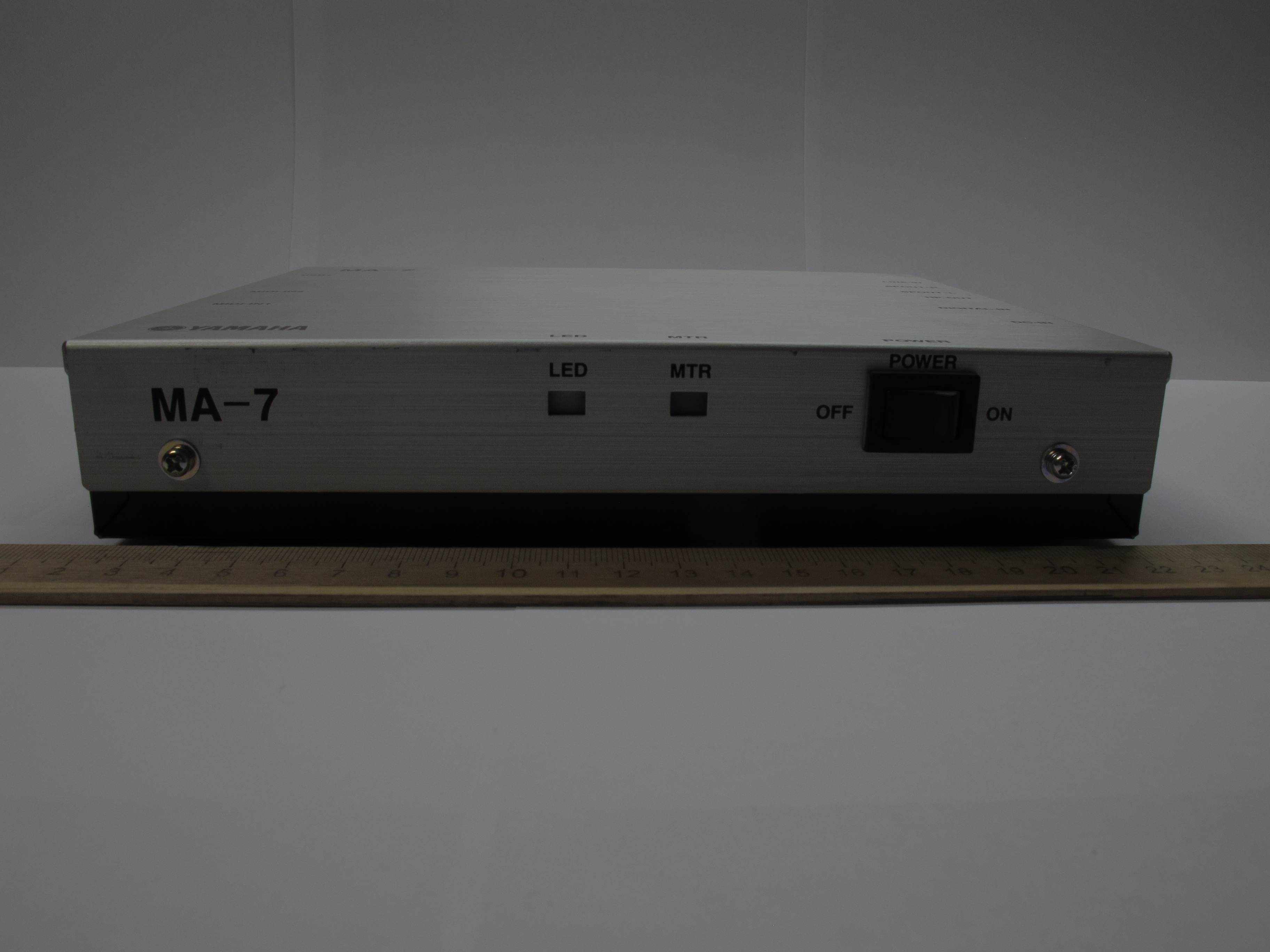
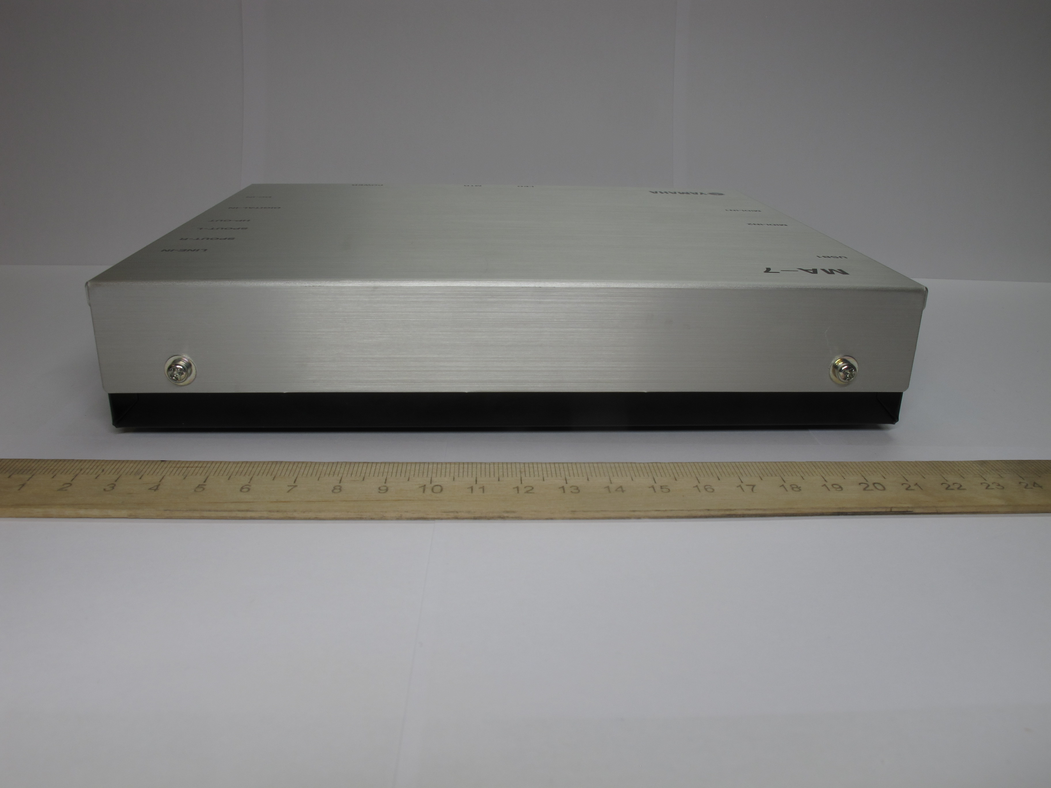
| The dev board right side. |
 |
|---|
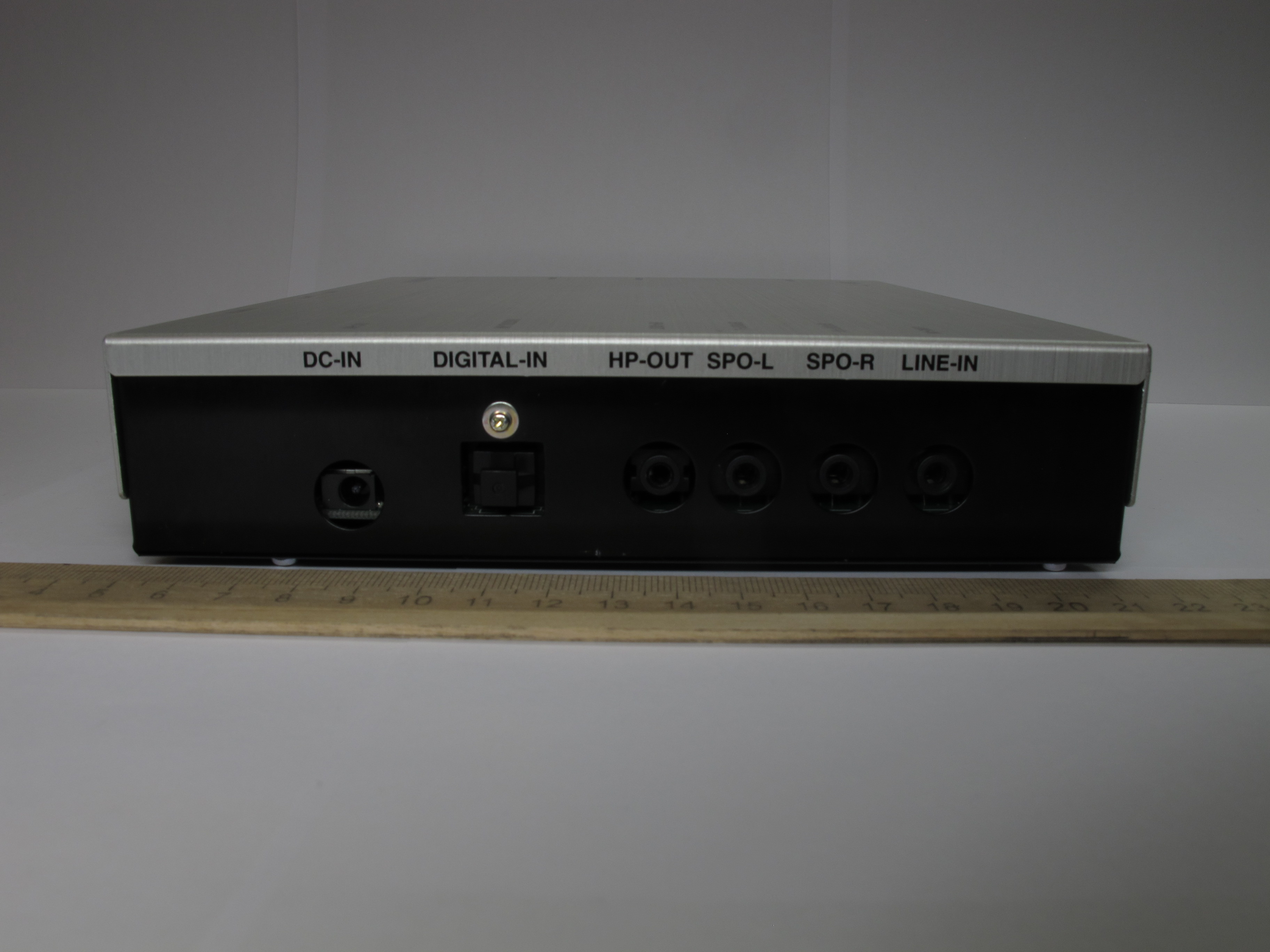
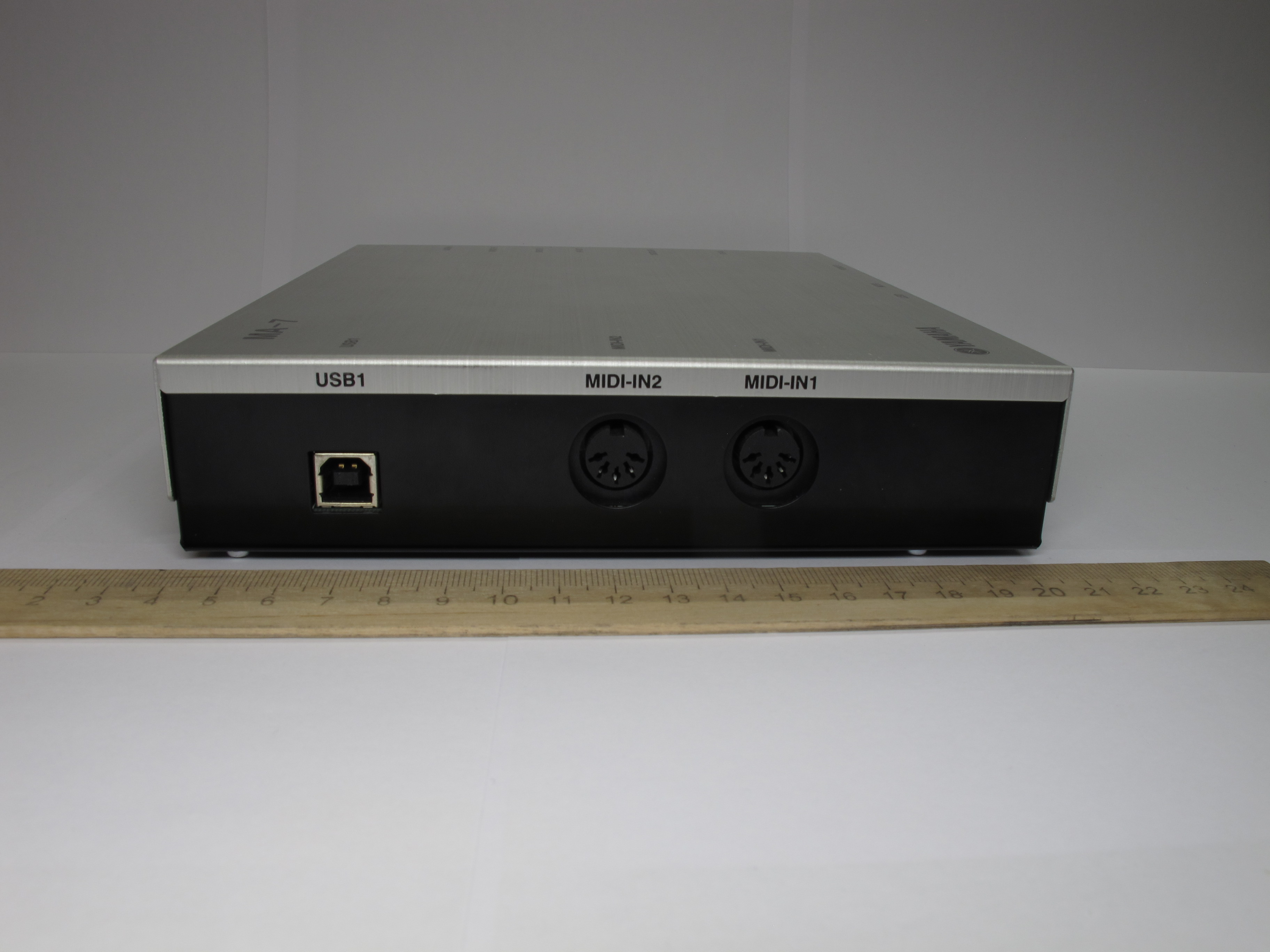
| The dev board back side. |
 |
|---|
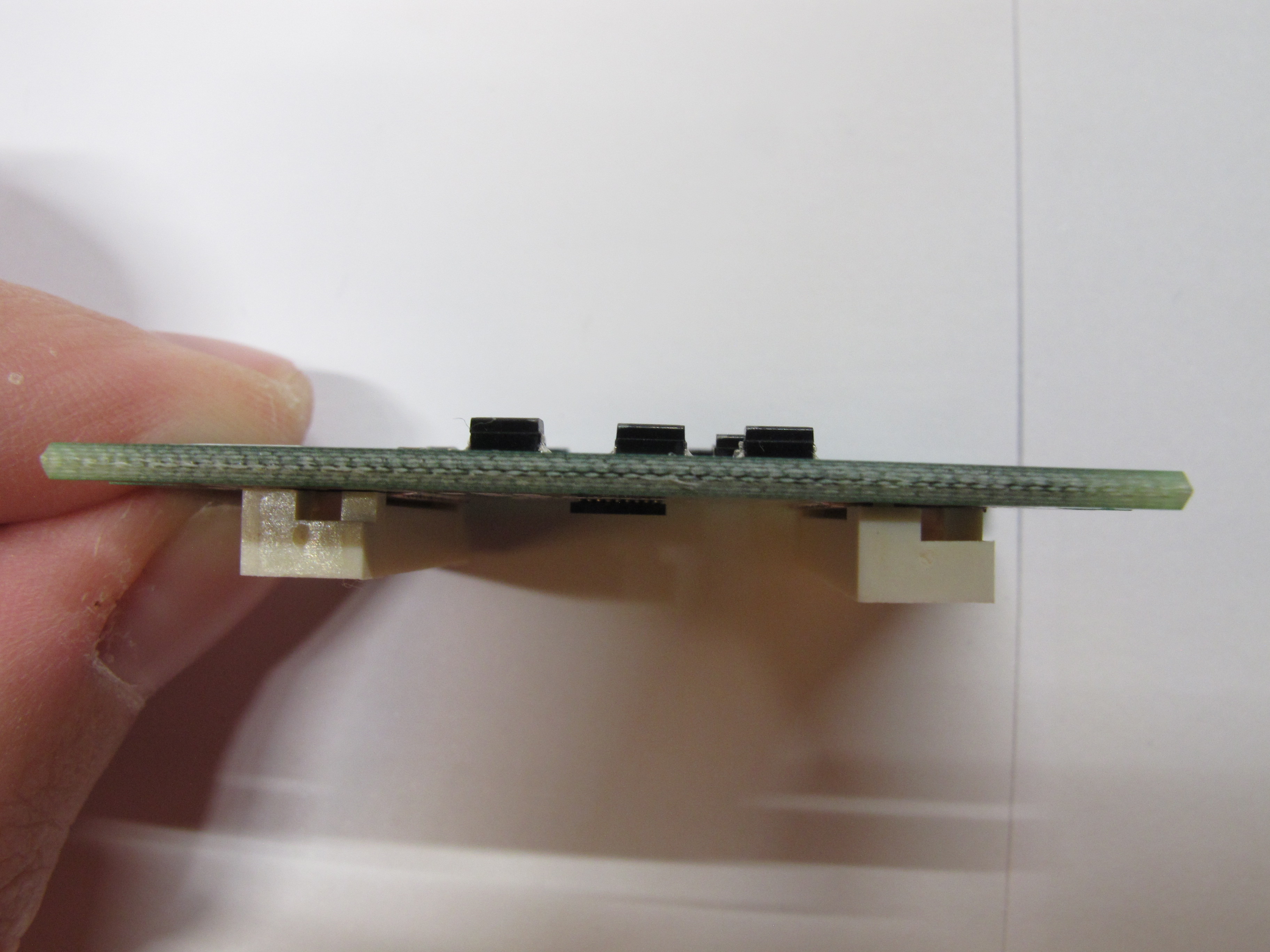
| The dev board left side. |
 |
|---|
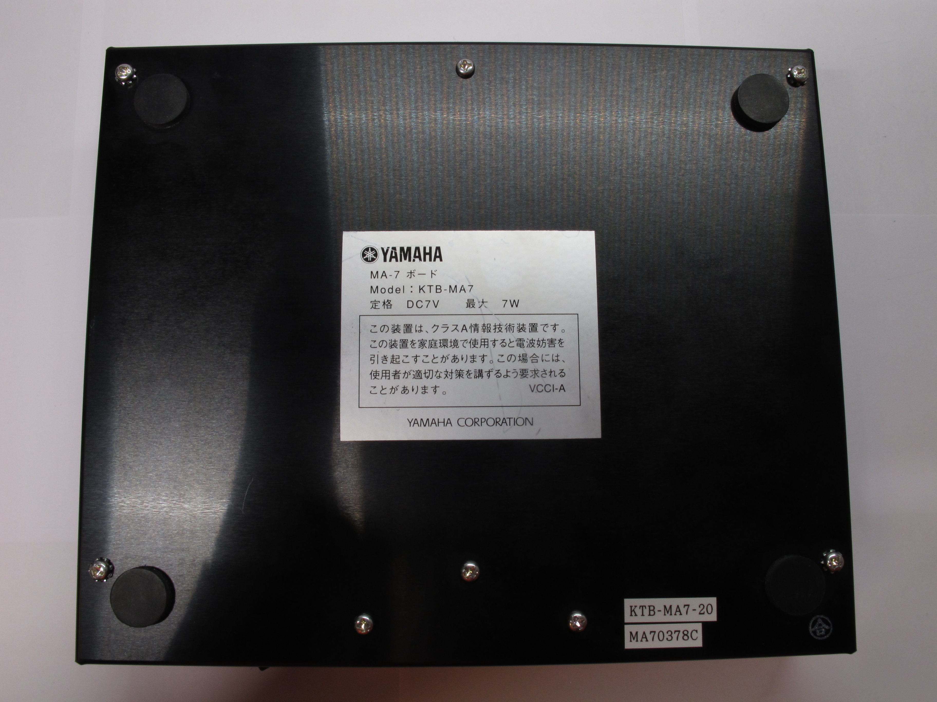
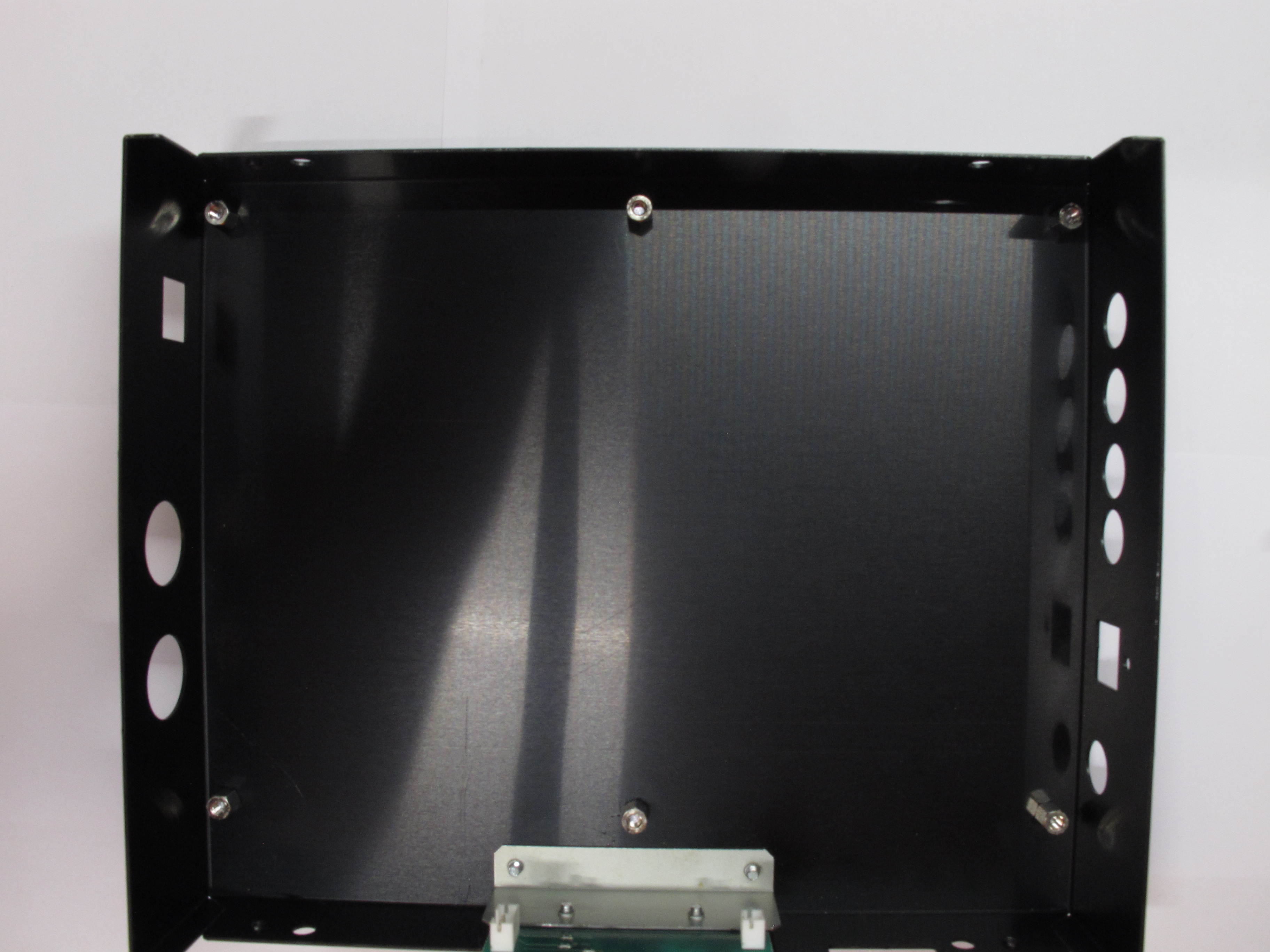
| The dev board belly. |
 |
|---|
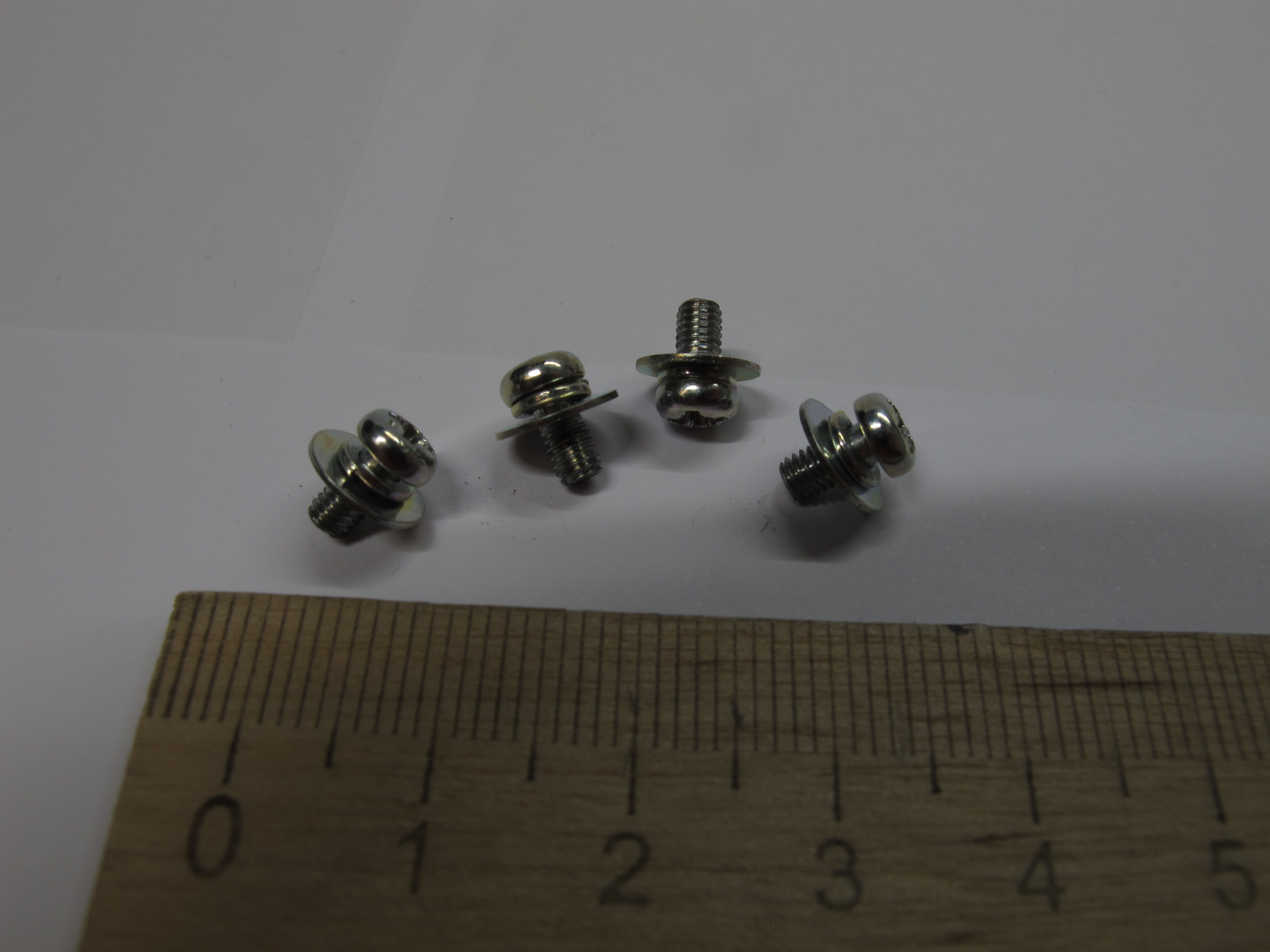
| Four screws that hold the upper lid. |
 |
|---|
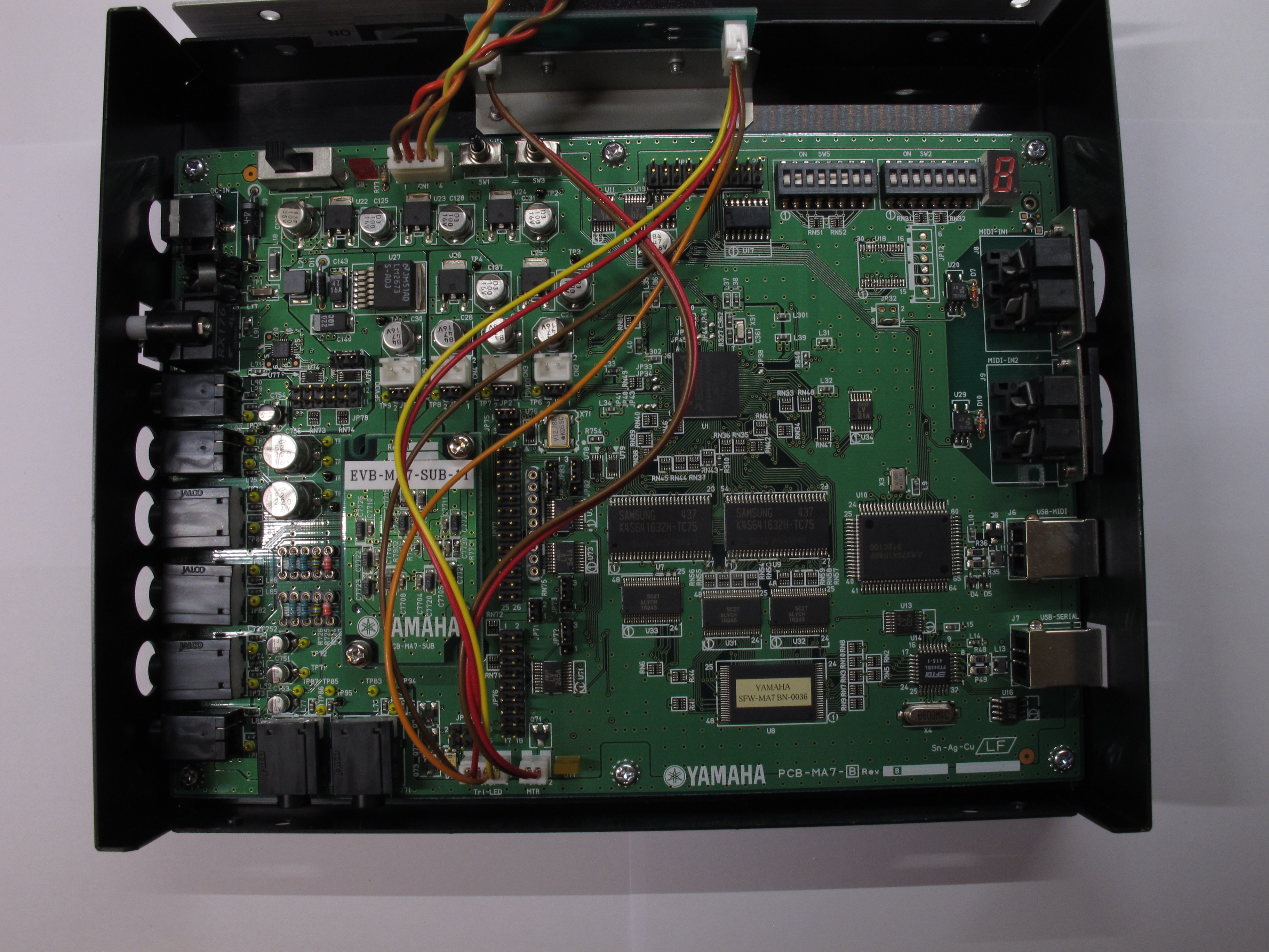
| Upper lid removed. |
 |
|---|
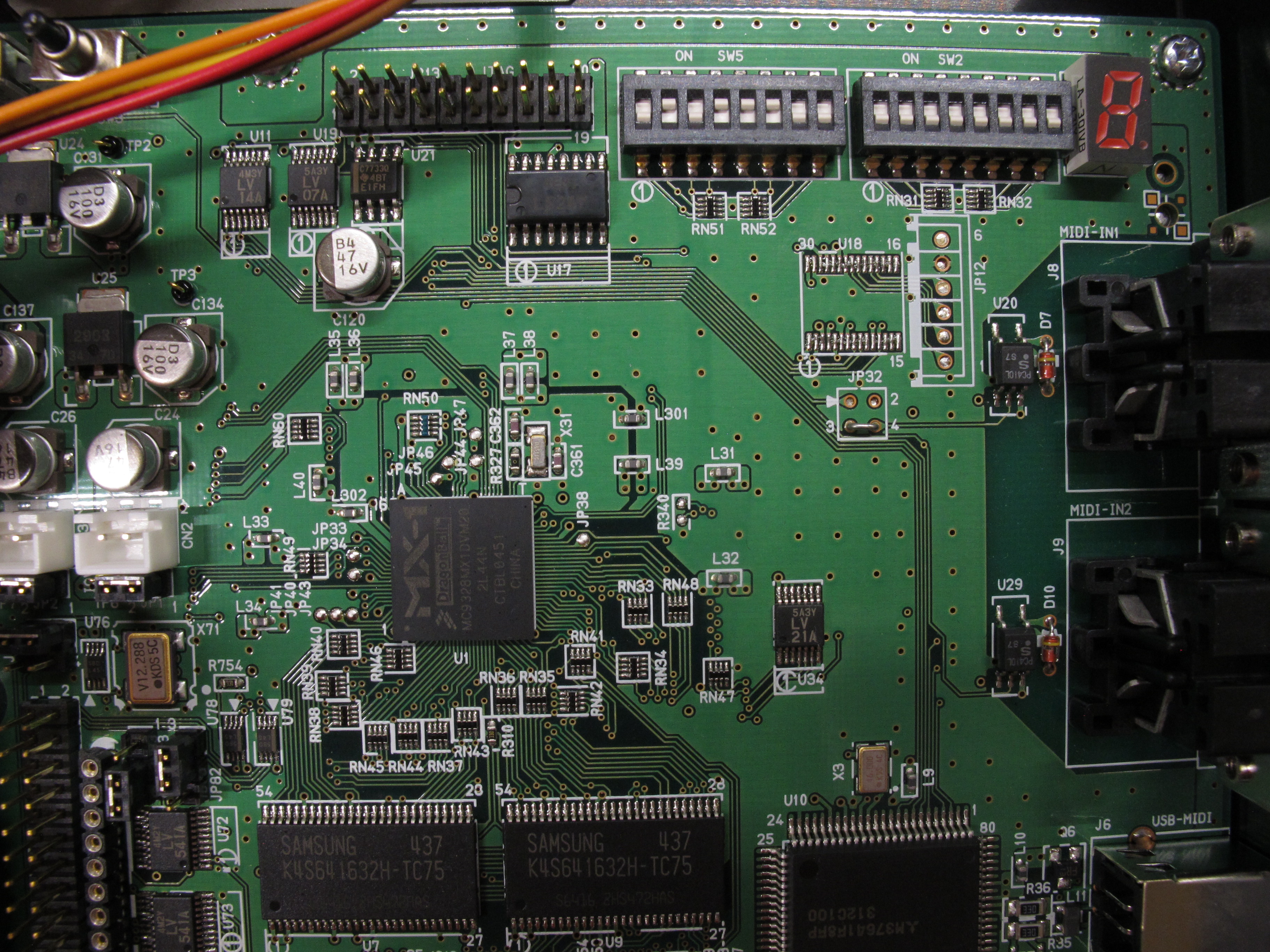
| Board's PCB full shot, top side. |
 |
|---|
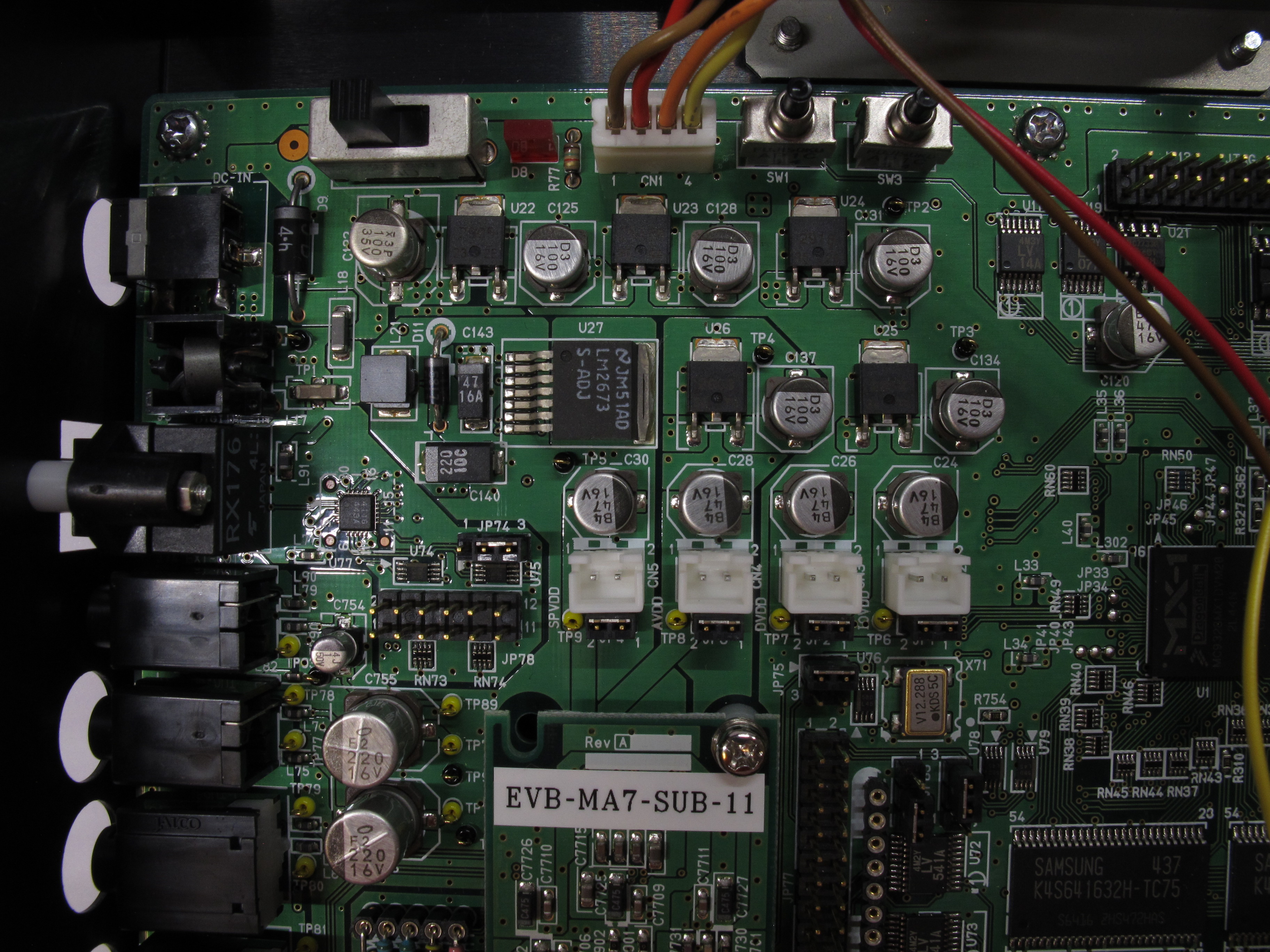
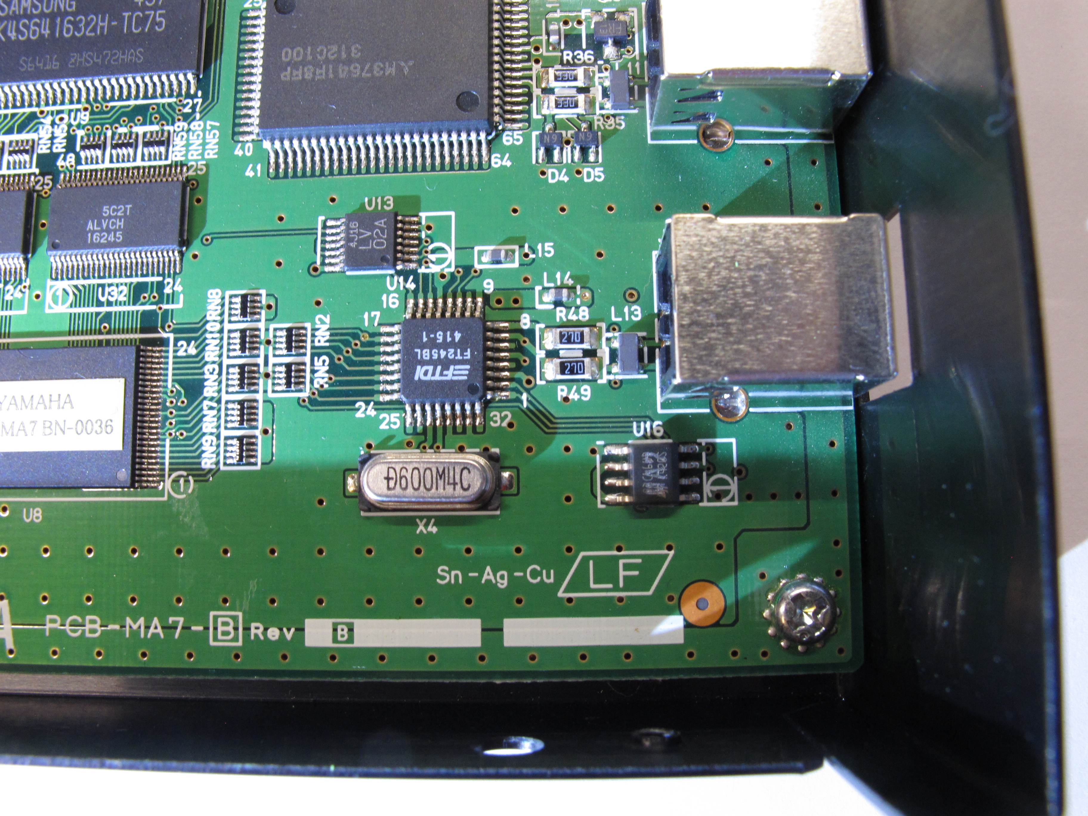
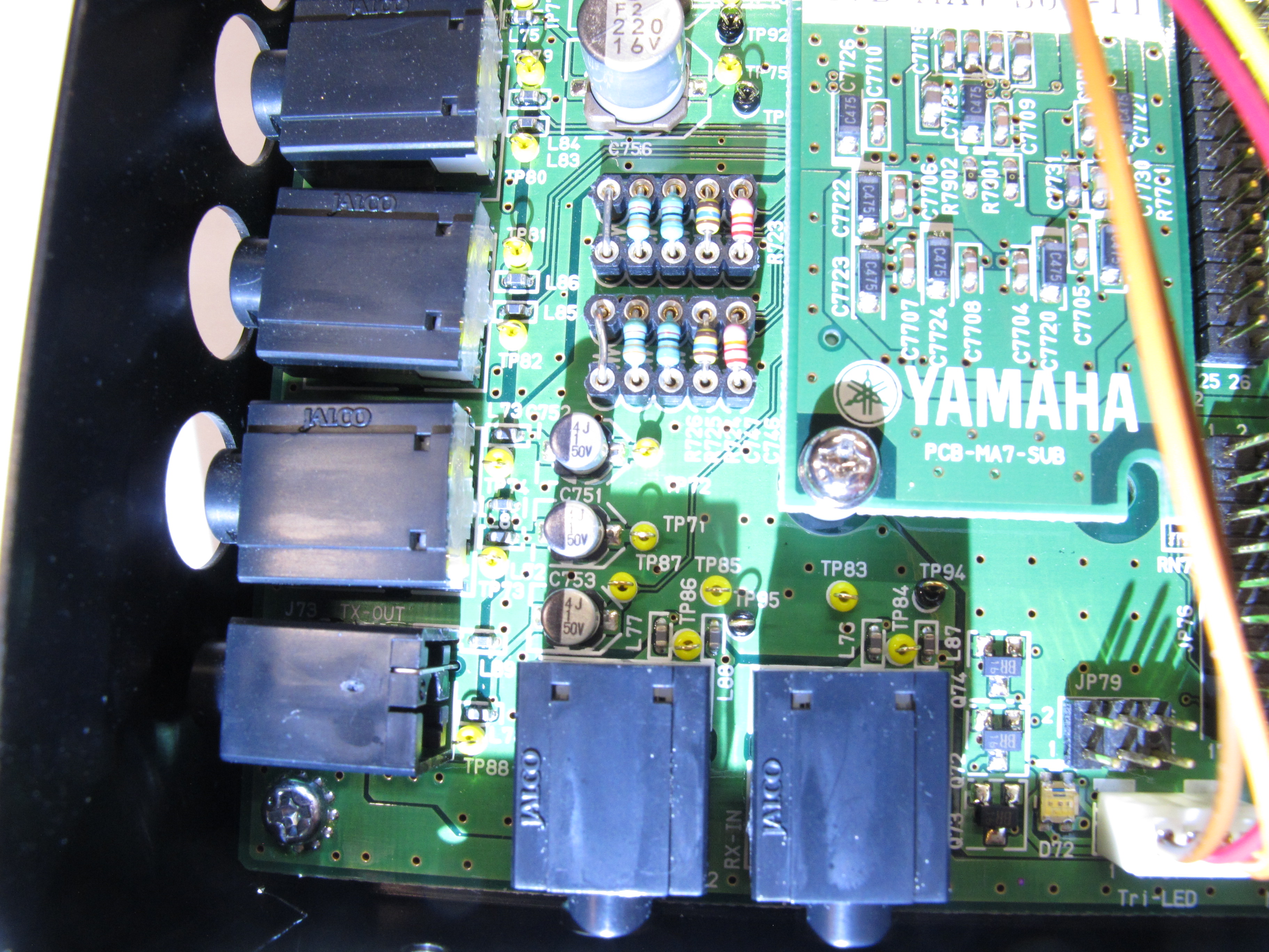
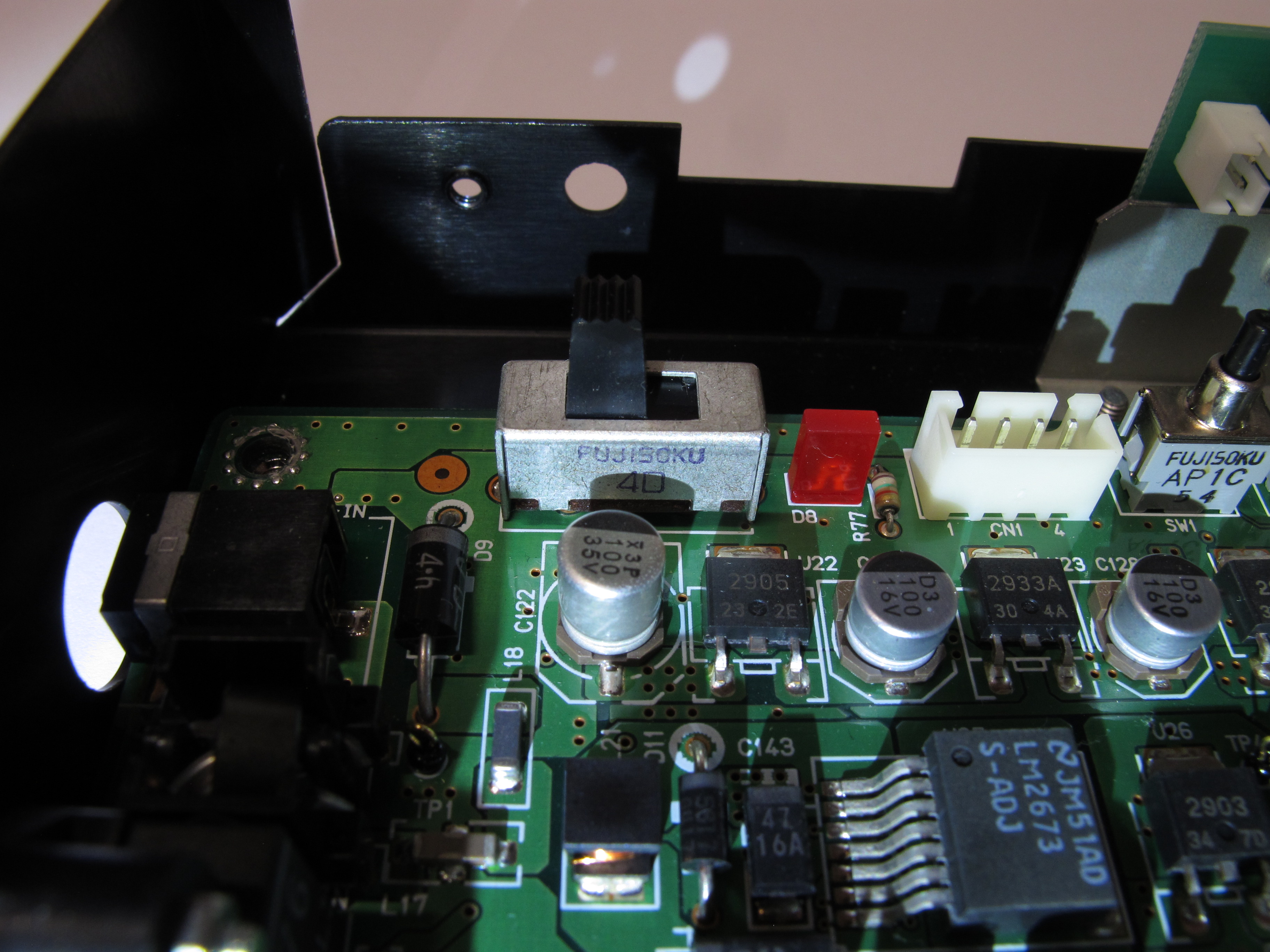
| Board's PCB upper left corner. You can already see that one jack does not have a hole for it. Also the whole board has A LOT of test points and 0-resistance resistors... |
 |
|---|
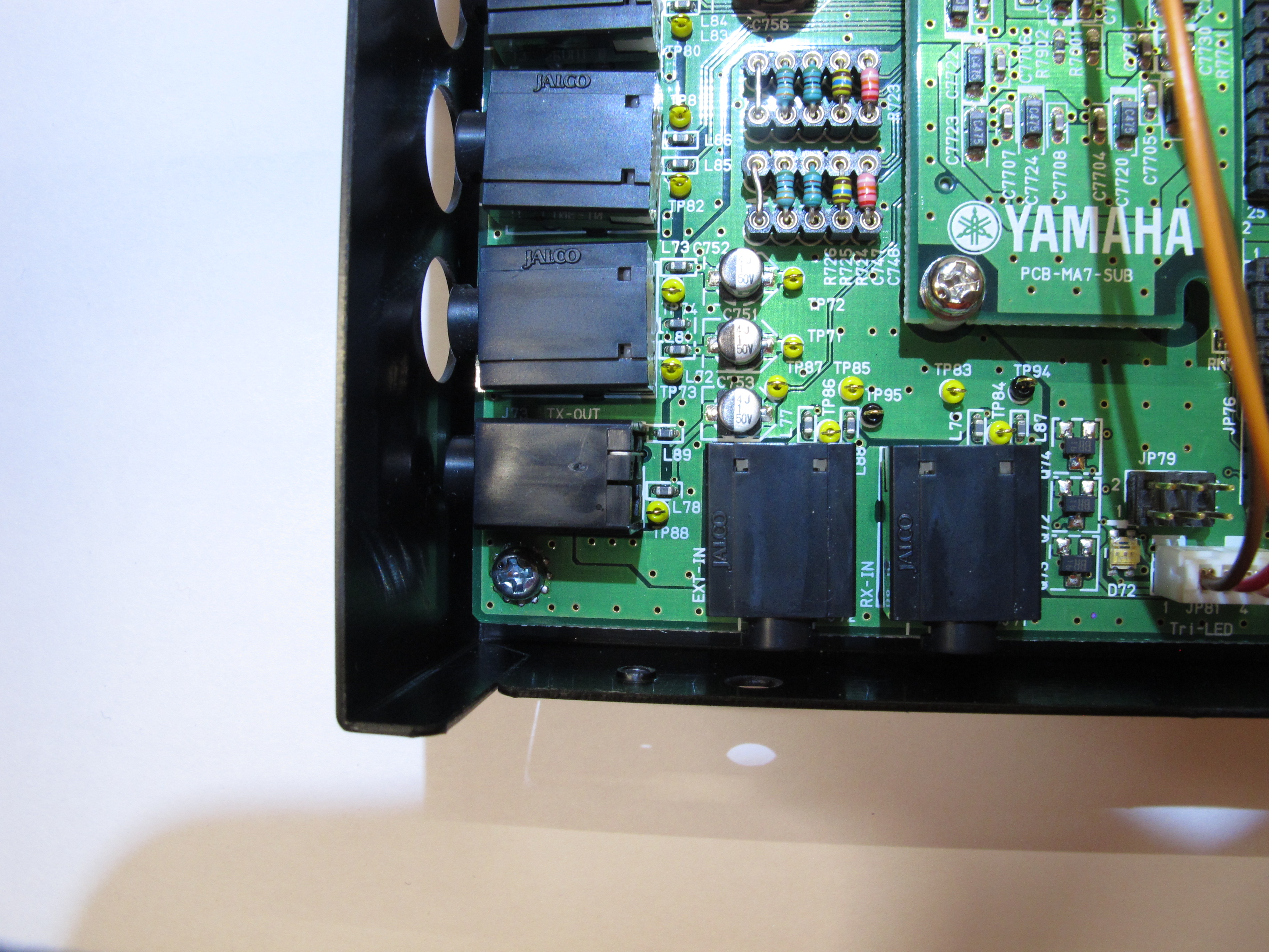
| Board's PCB bottom left corner. |
 |
|---|
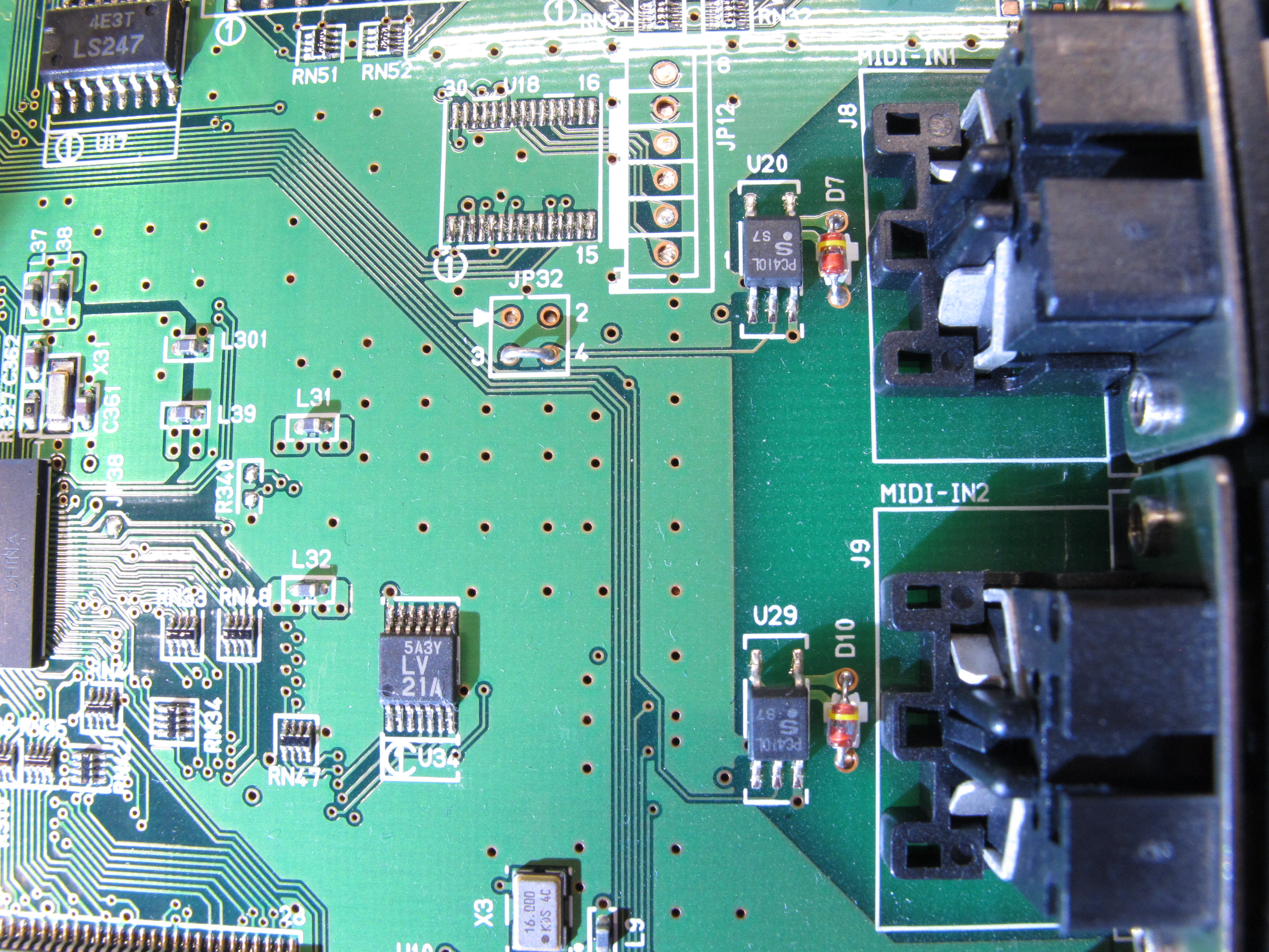
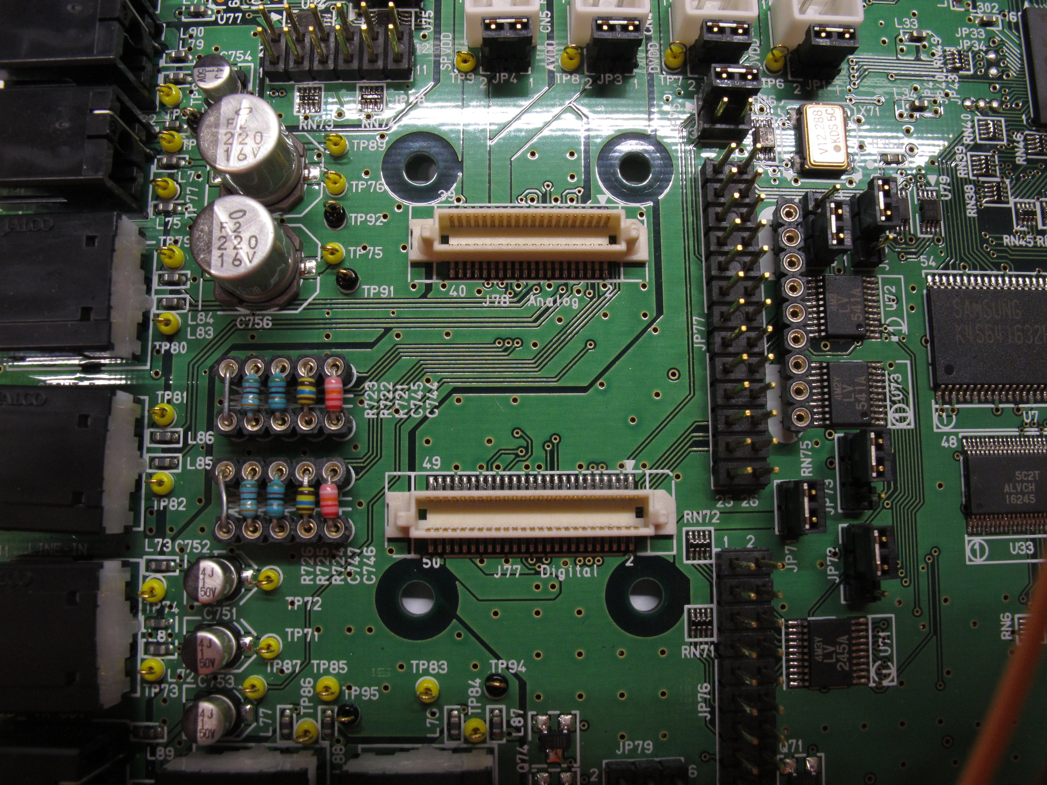
| Board's PCB upper right corner. |
 |
|---|
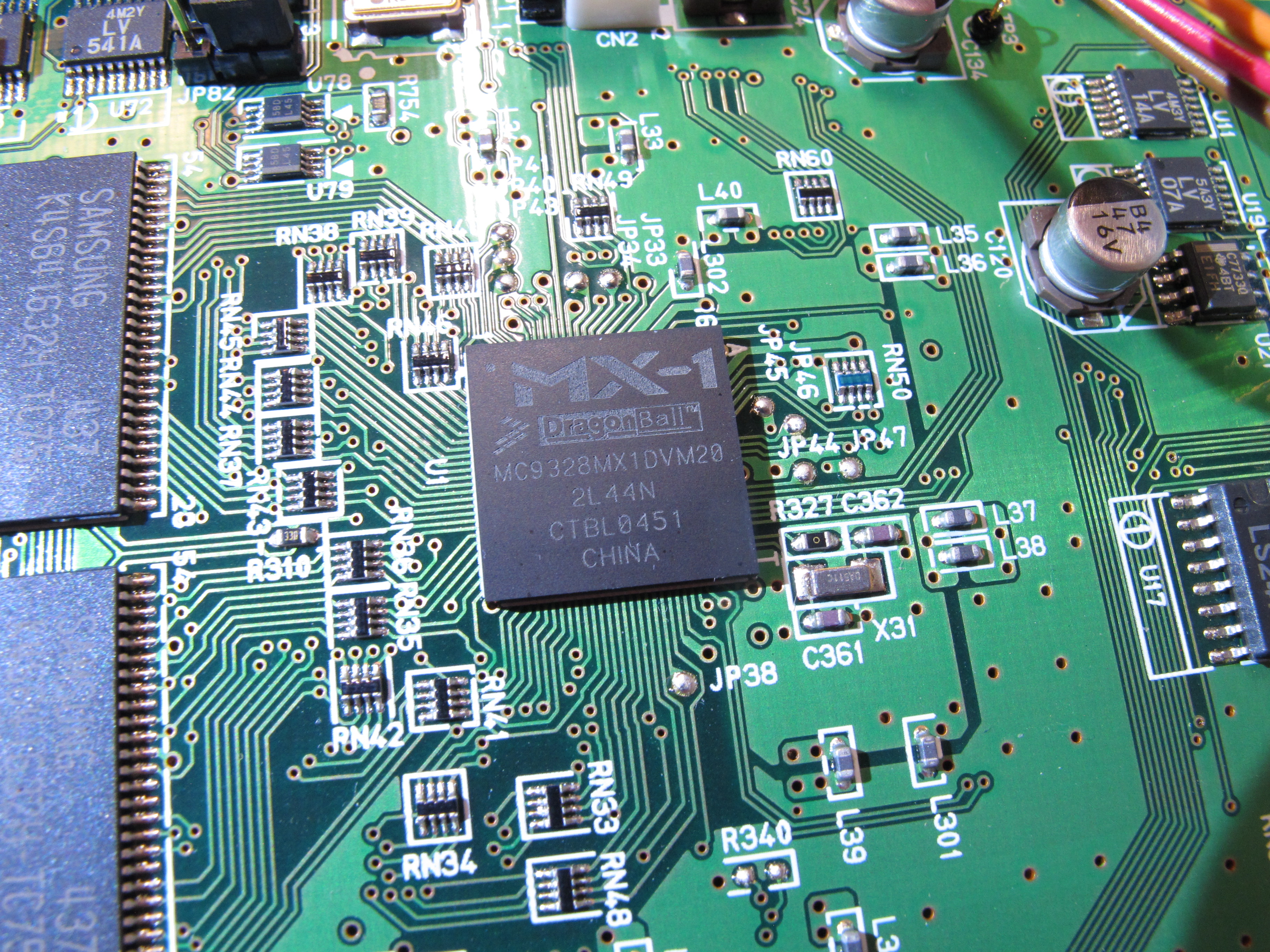
| The CPU on the dev board. It, along with RAM, ROM etc. simulates the mobile phone chip is connected to. And yes, only now I started using a flashlight to make reading chip markings easier. |
 |
|---|
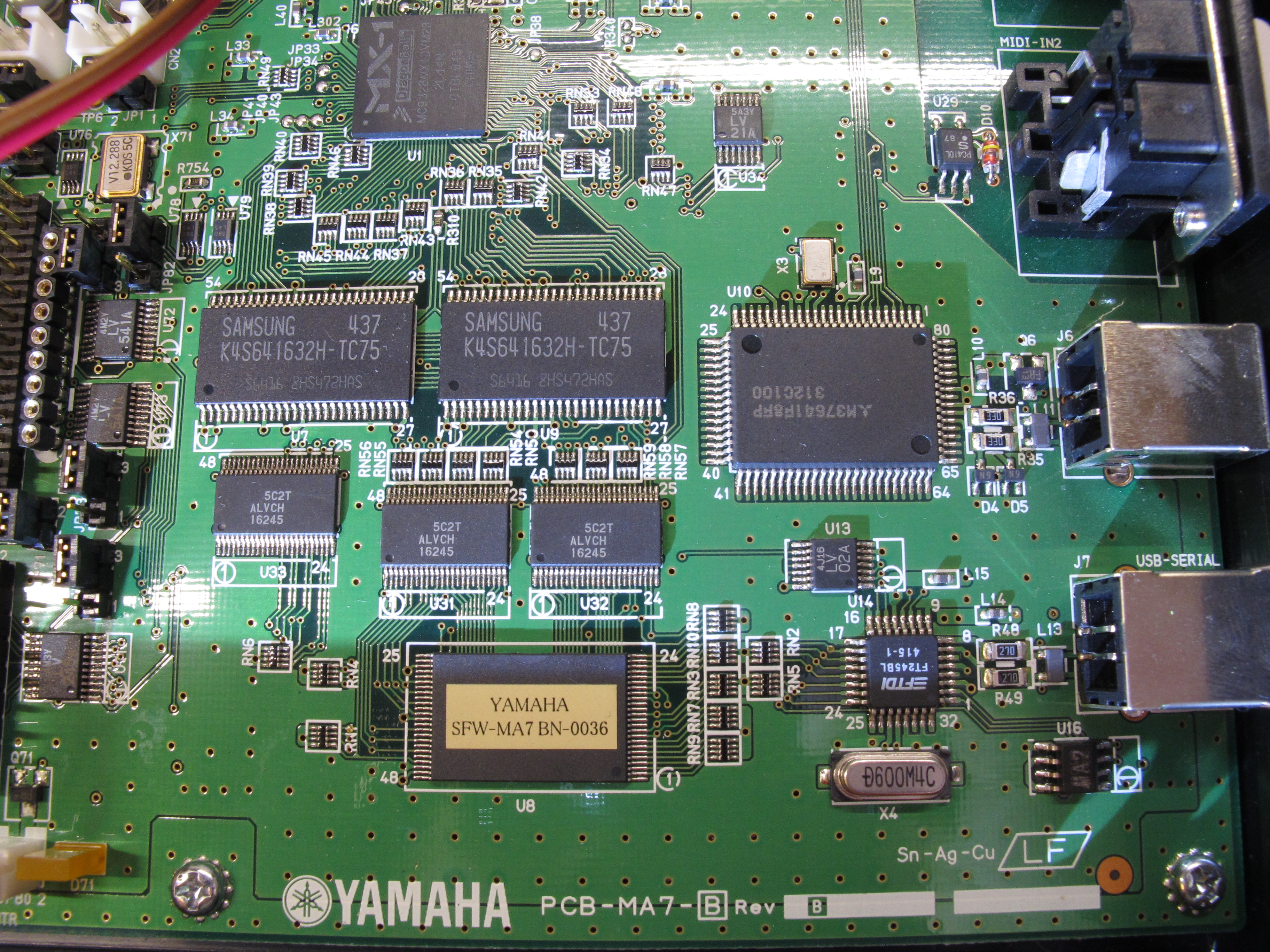
| Two RAM units, 16 MiB each. To the right from them is another 8-bit microcomputer, idk why. The chip with yellow-ish label is probably the ROM. |
 |
|---|
| Another shot so that markings on small chips are easier to read. |
 |
|---|
| And another. |
 |
|---|
| And another. |
 |
|---|
| And another, this time closer to the top. |
 |
|---|
| And another, this time for the components on which markings are on their vertical surfaces. |
 |
|---|
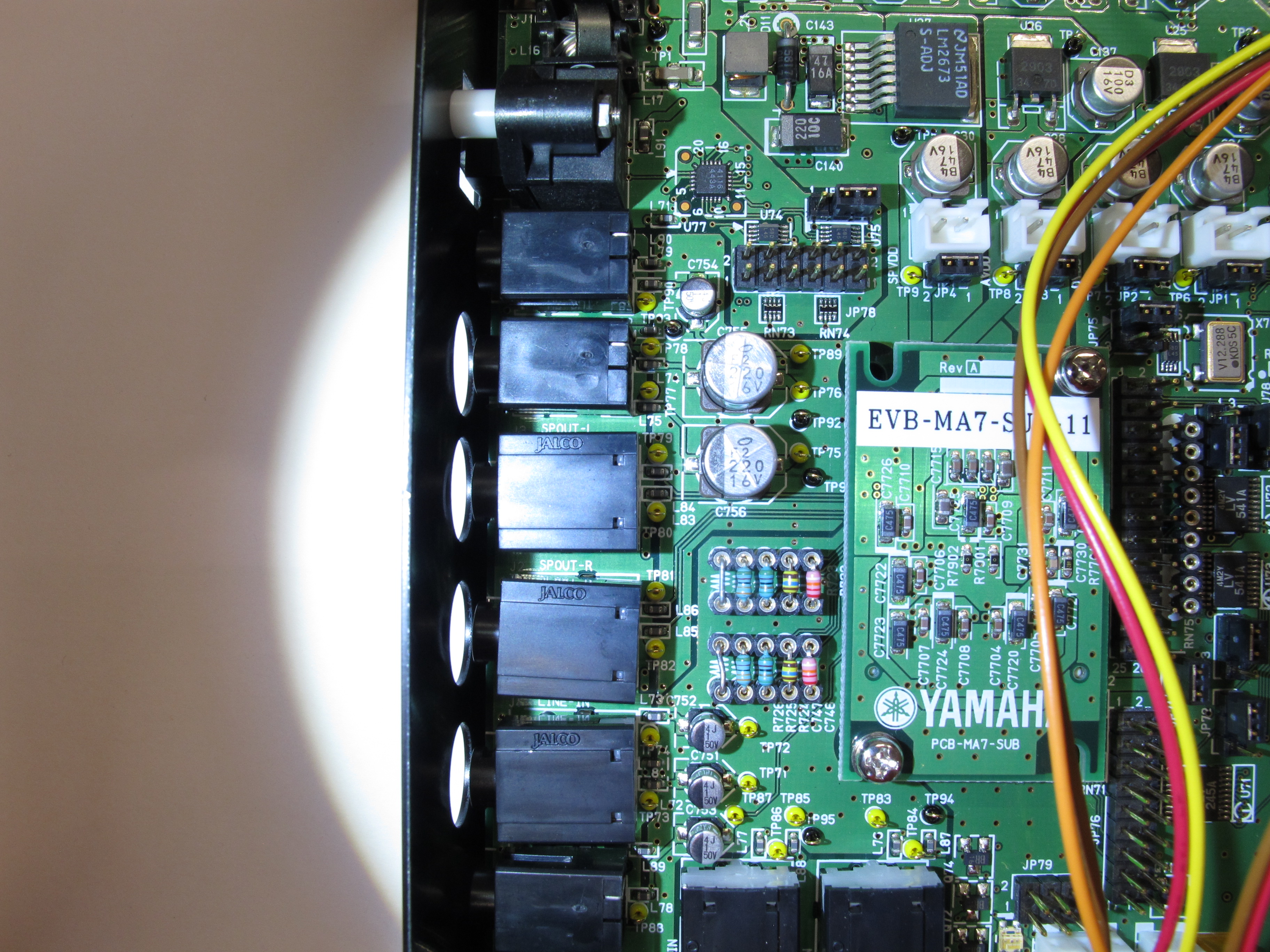
| Silkscreen labels of audio jacks. |
 |
|---|
| More silkscreen labels of audio jacks. |
 |
|---|
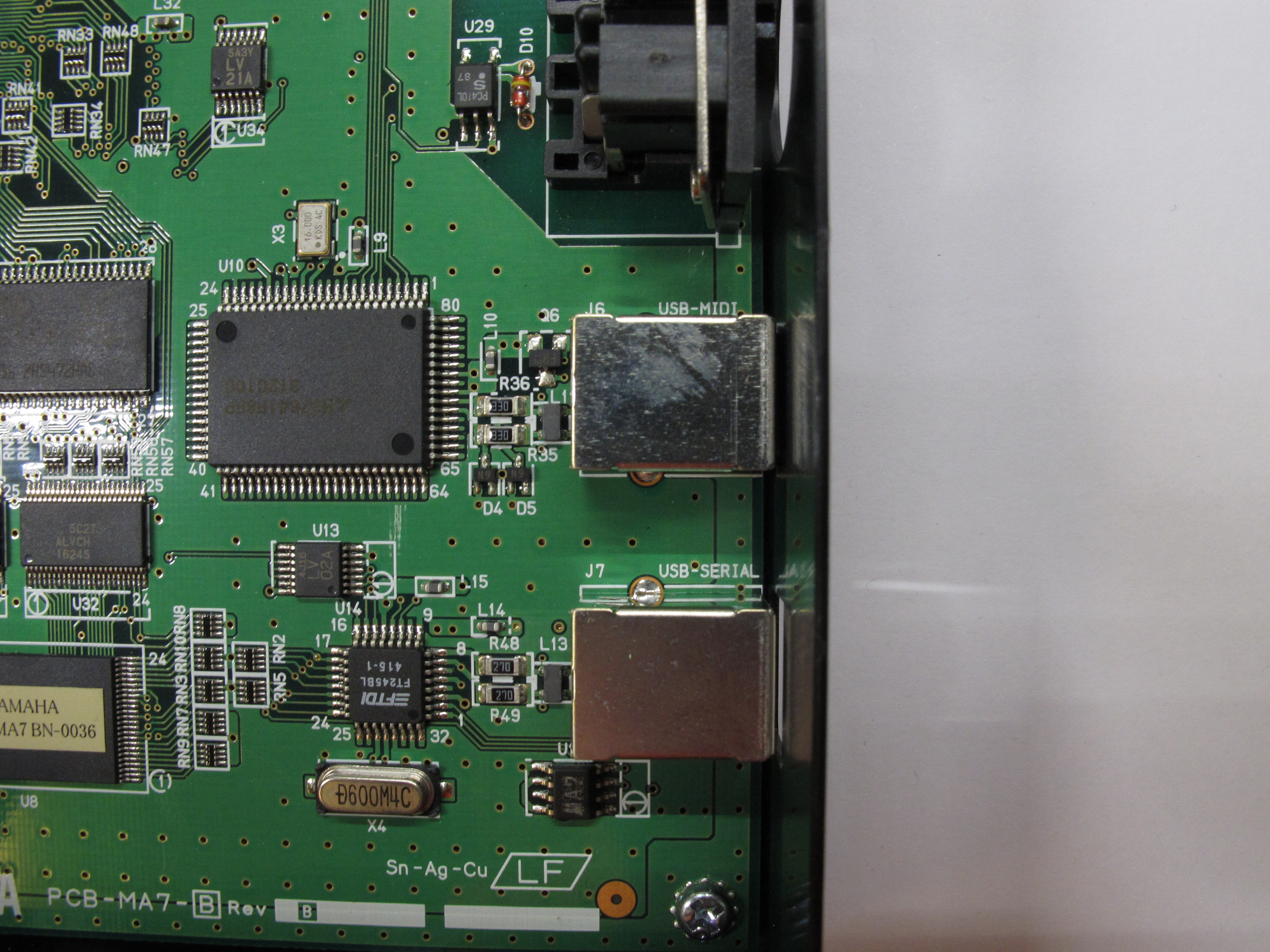
| Silkscreen labels of USB ports. |
 |
|---|
| We need to know who manufactured the jacks. |
 |
|---|
| And power switch. |
 |
|---|
| And these two things. |
 |
|---|
| More silkscreen labels with stellar lighting. |
 |
|---|
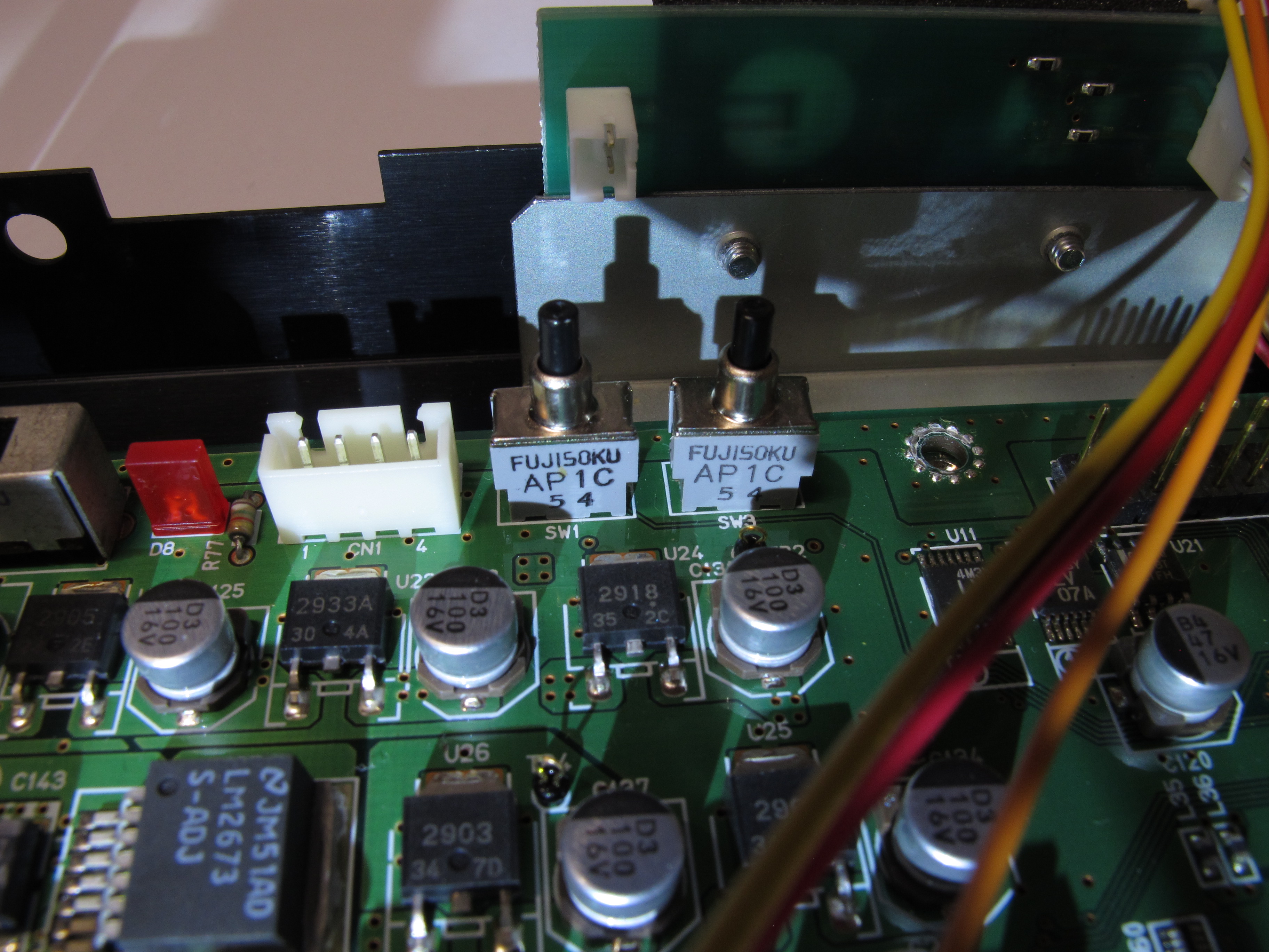
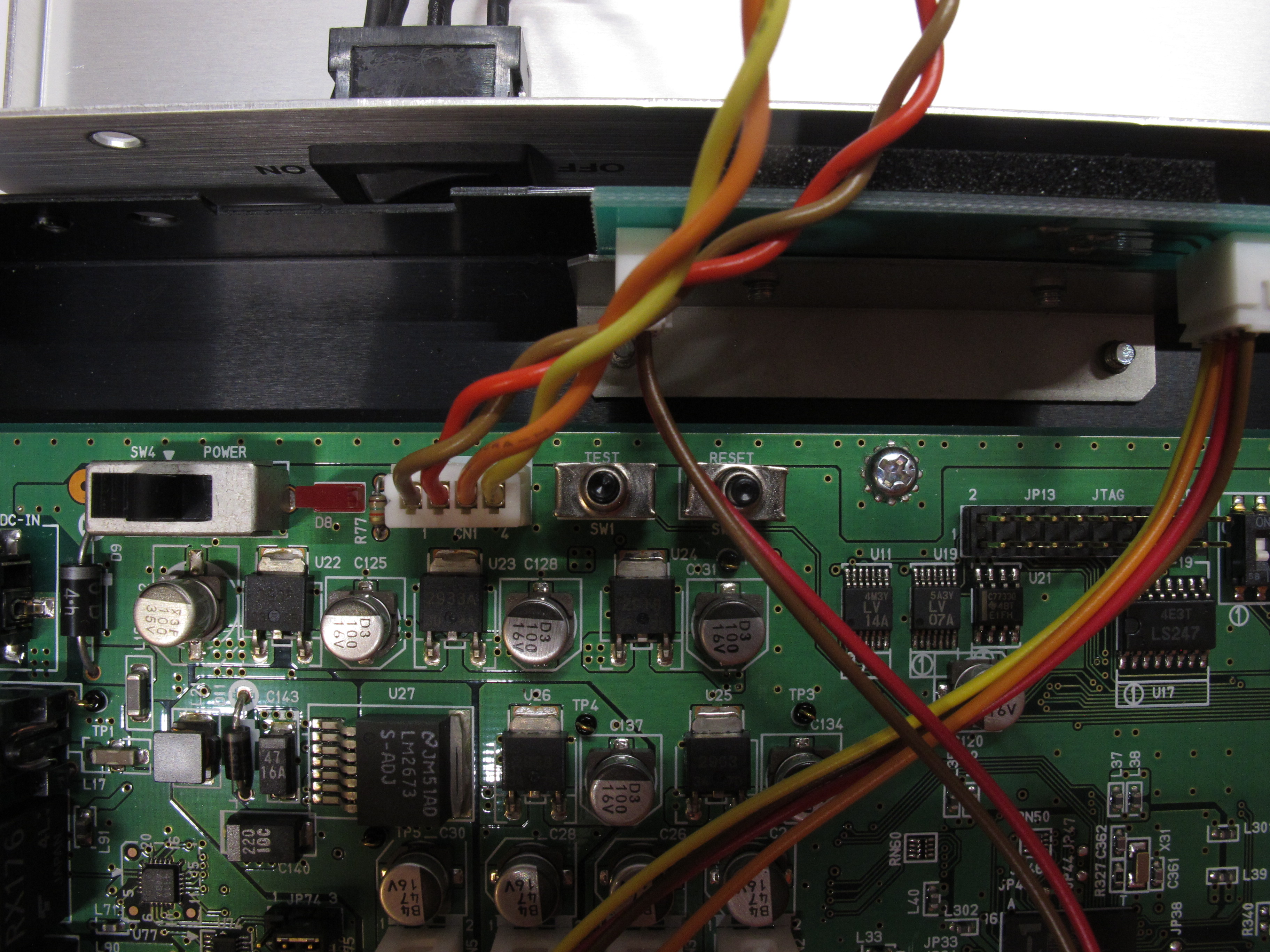
| Silkscreen labels of switches. |
 |
|---|
| I would have never guessed what these are for, I am serious. |
 |
|---|
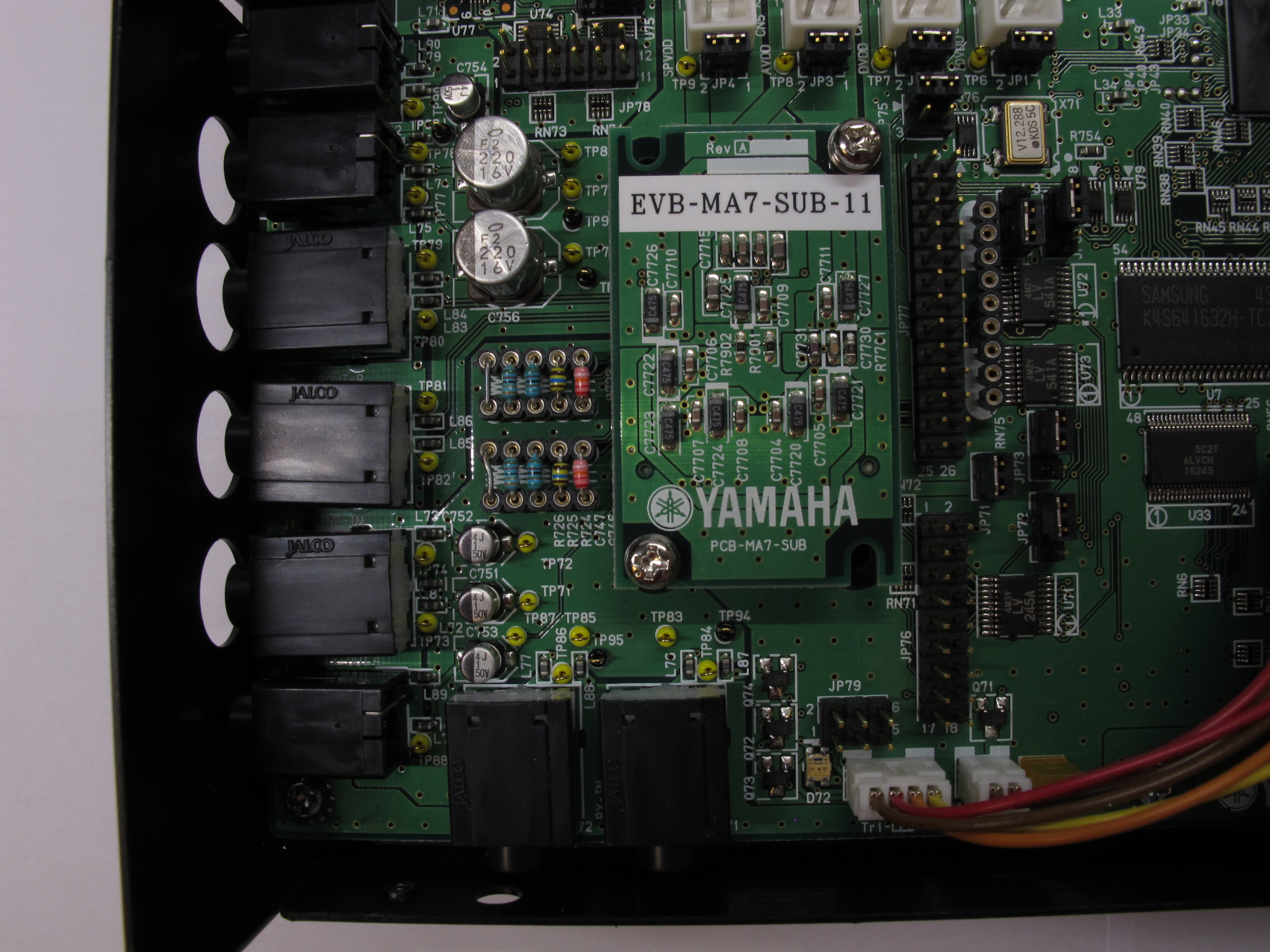
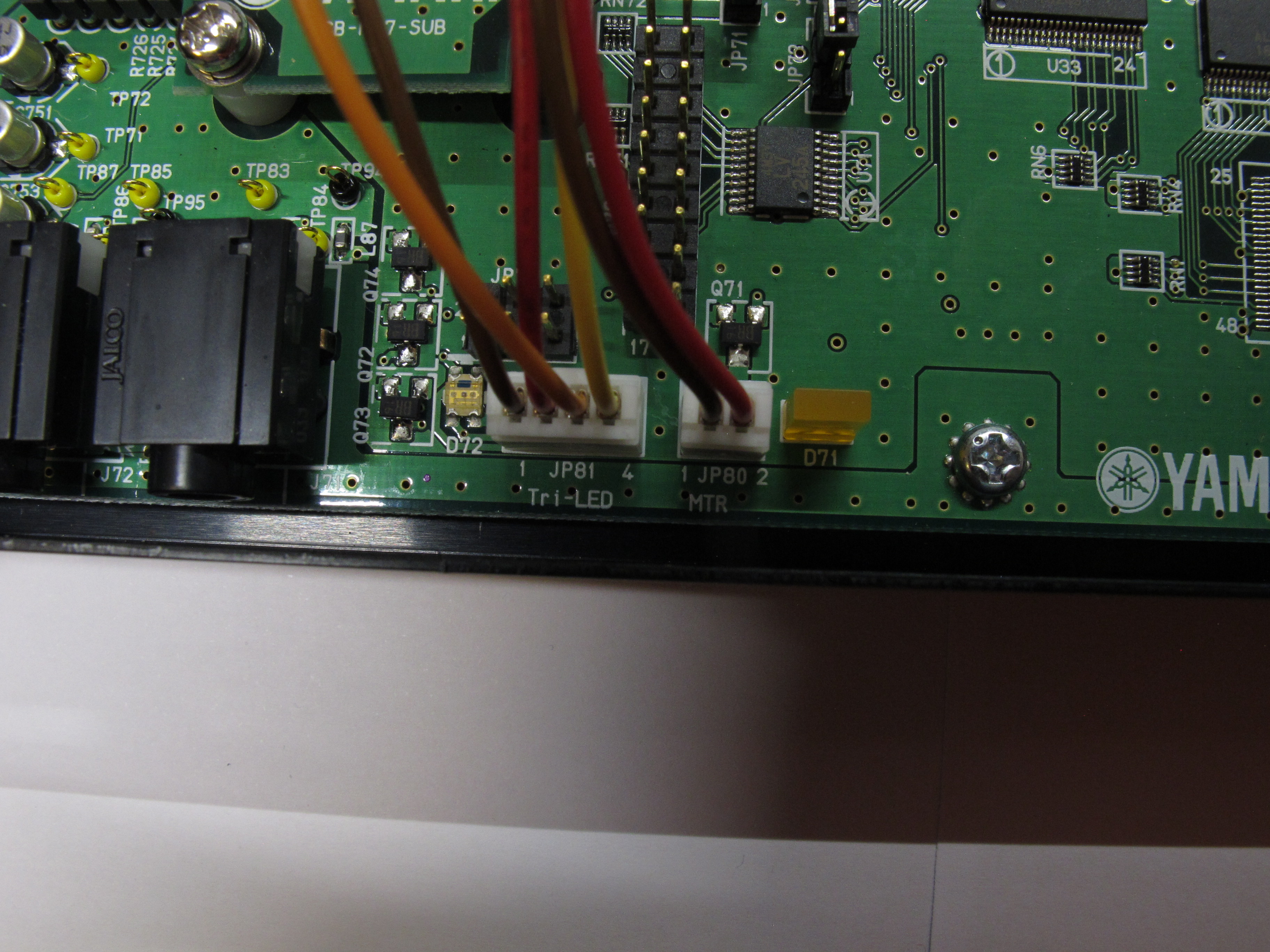
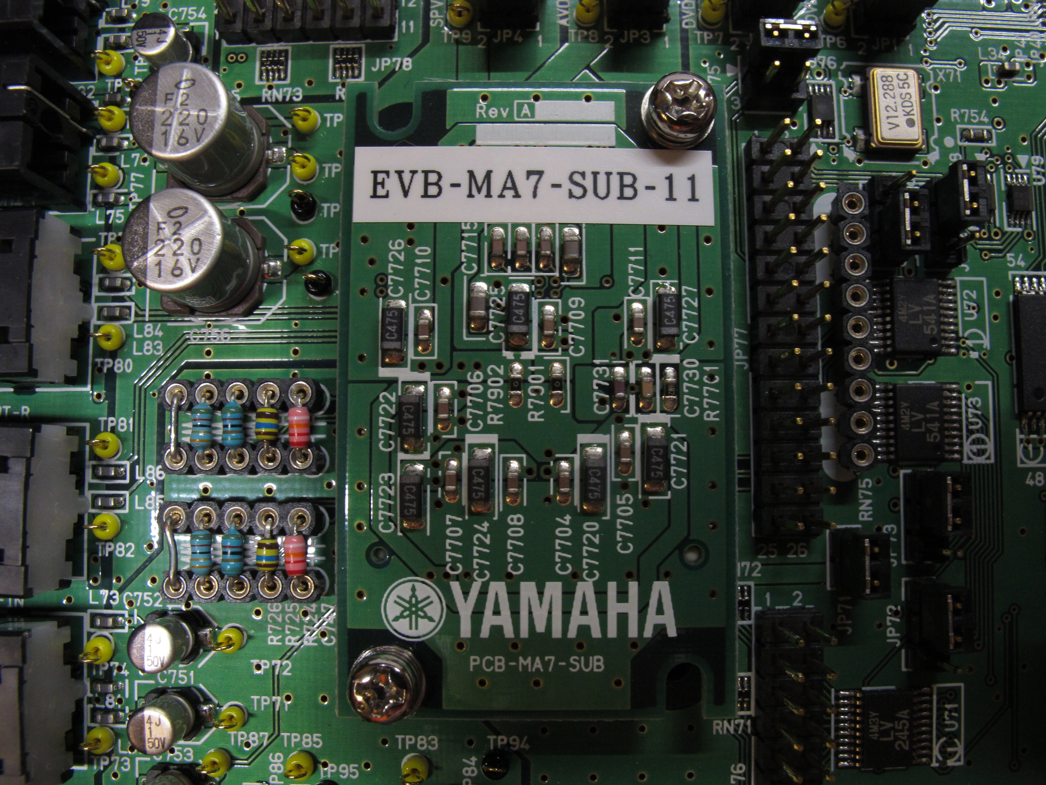
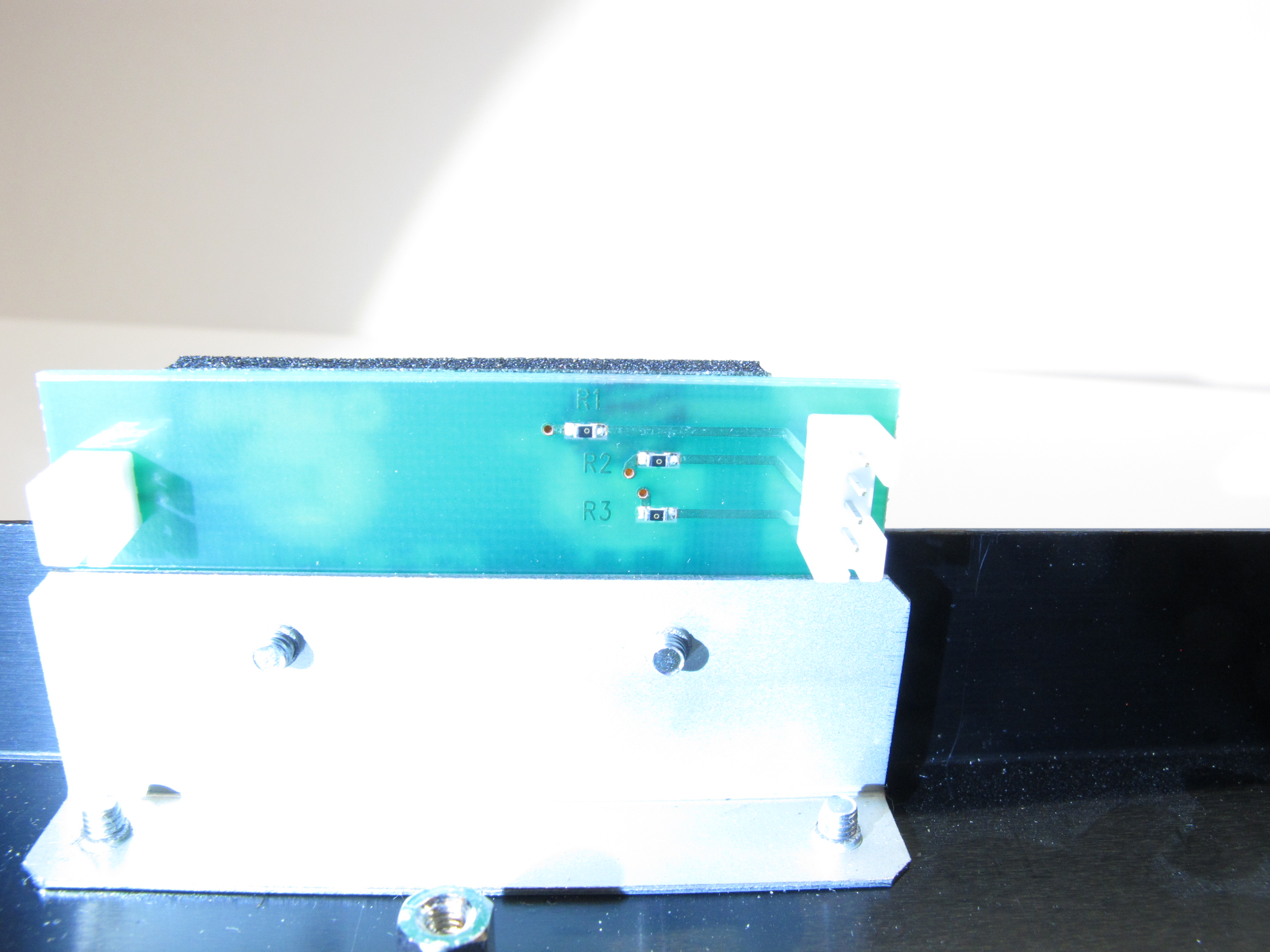
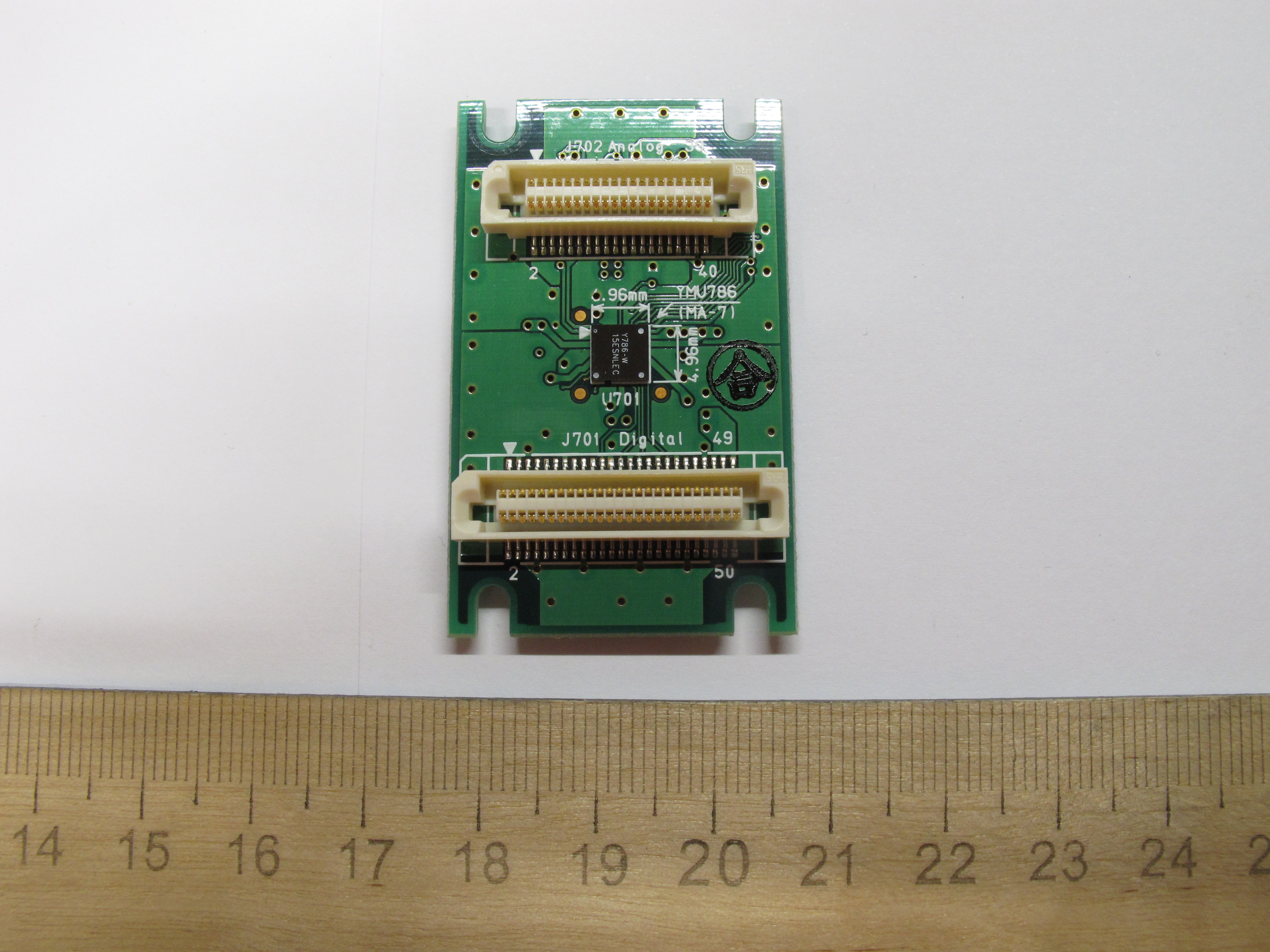
| A small elevated board which houses the actual MA-7 chip. |
 |
|---|
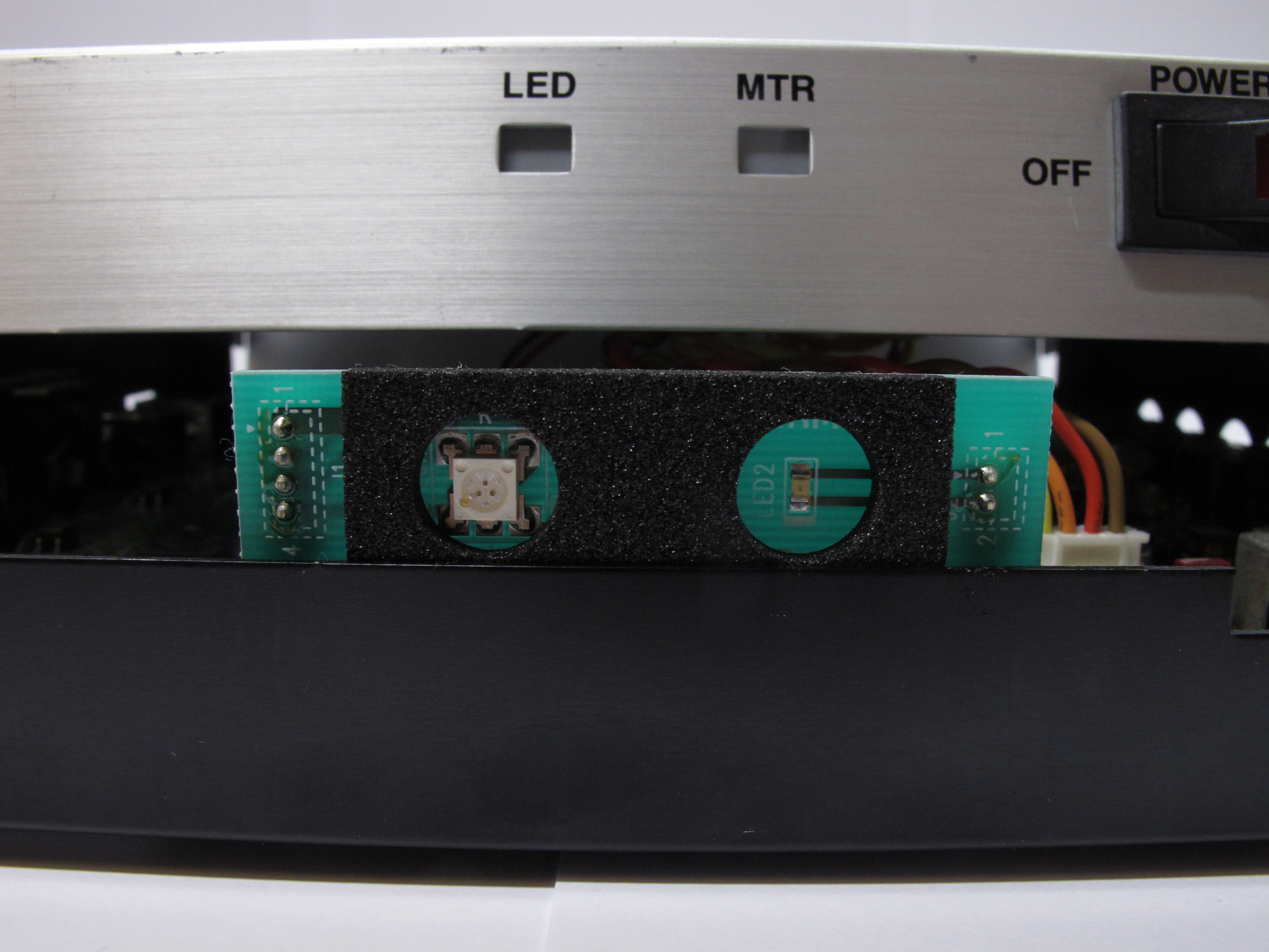
| Almost forgot to take a pic of LEDs panel. |
 |
|---|
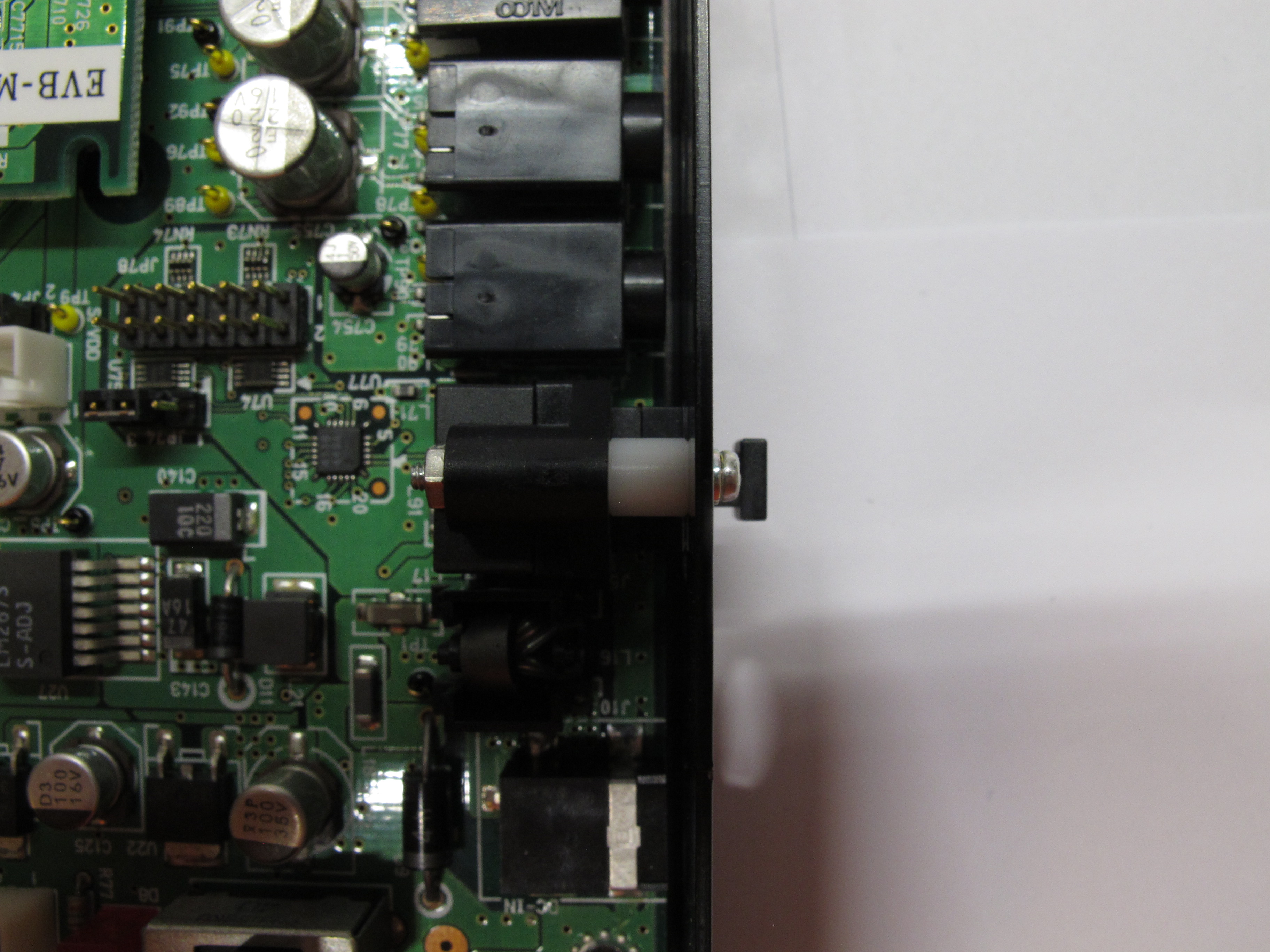
| The TOSLINK port is held in place by this screw. |
 |
|---|
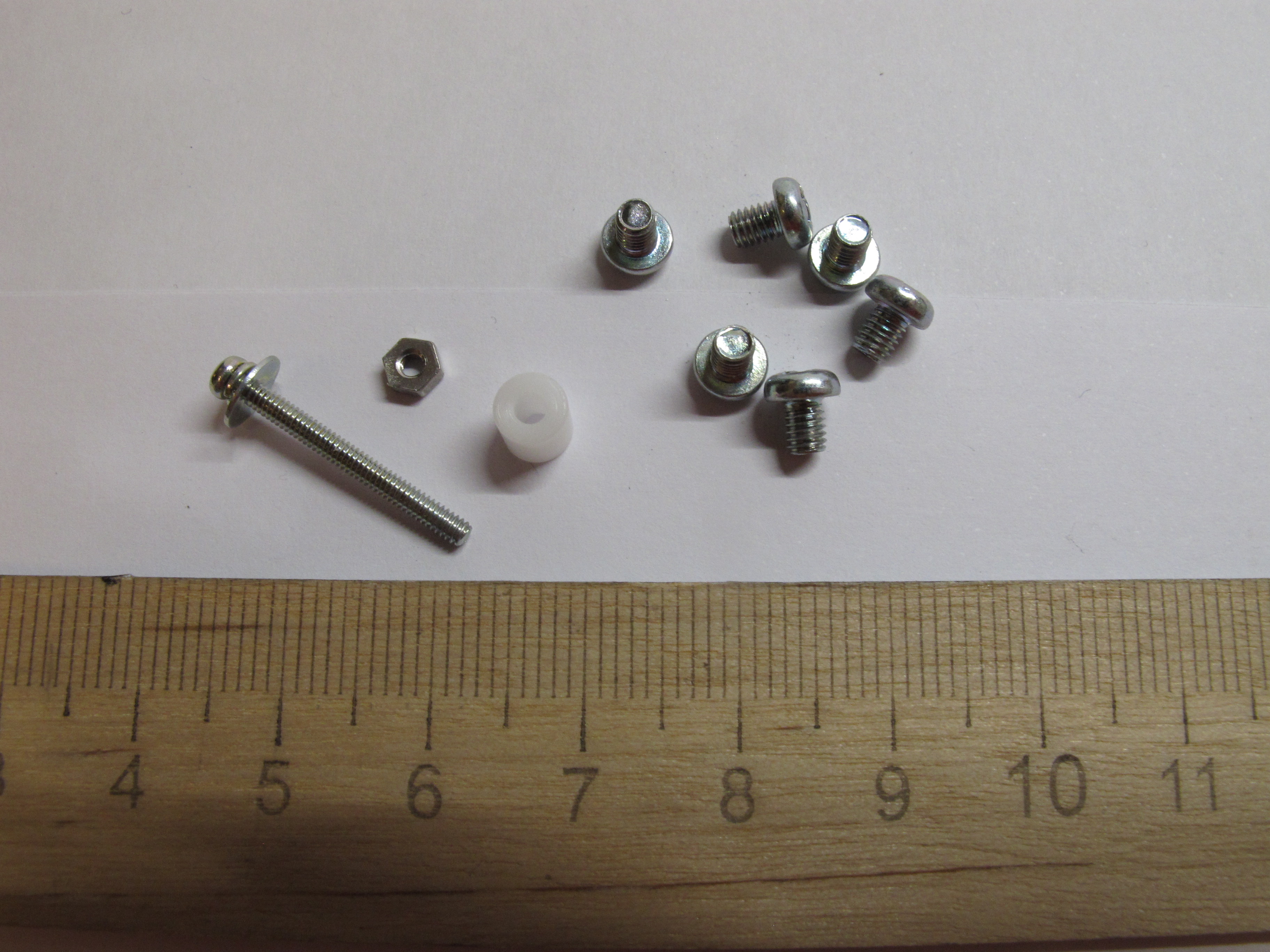
| Six screws holding the PCB in the case, and screw with nut and ughhhh plastic cylinder which holds the TOSLINK port. |
 |
|---|
| Empty case without the main PCB. |
 |
|---|
| Overlit backside of LEDs panel. |
 |
|---|
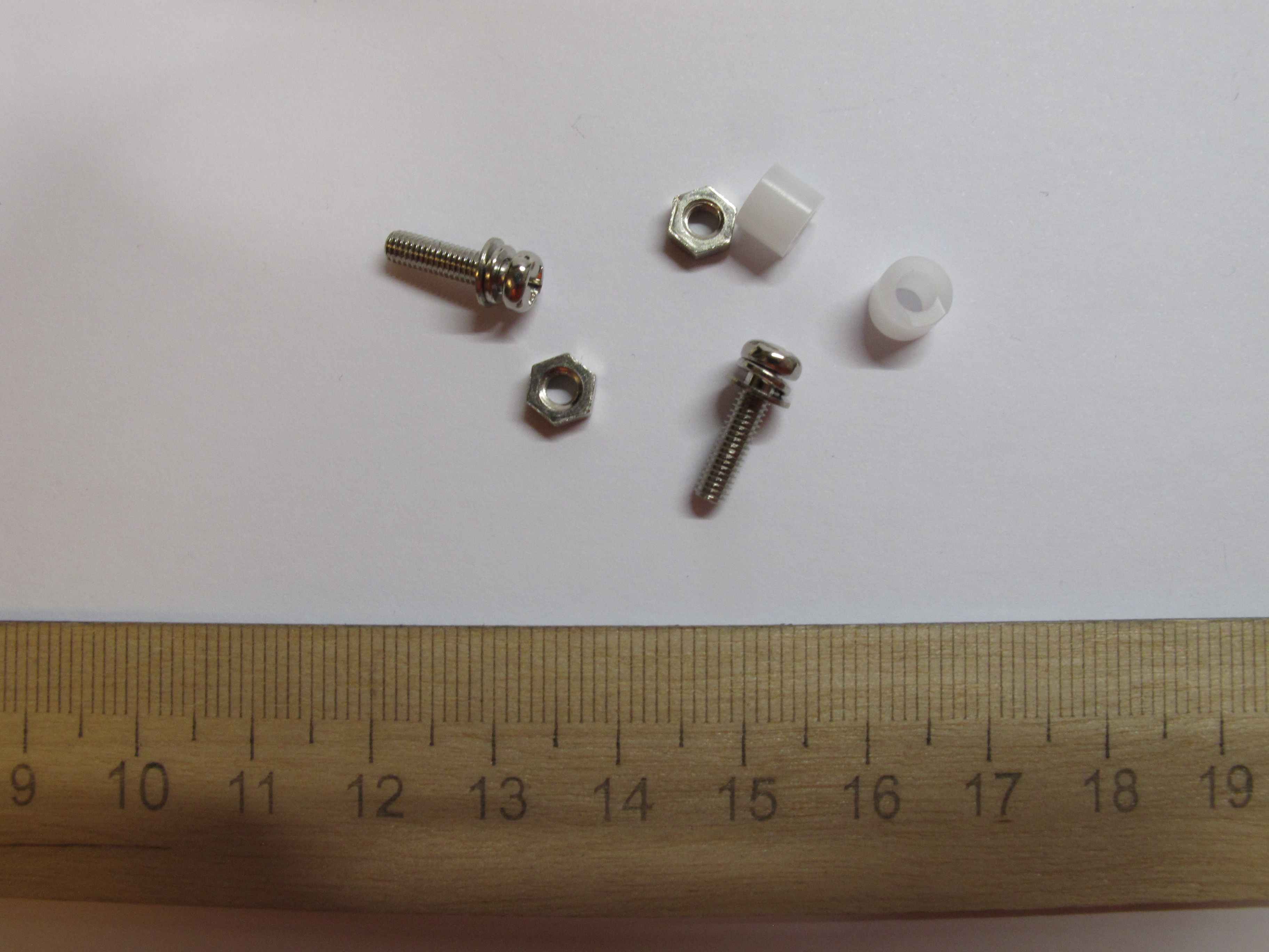
| These two screws with nuts hold the small elevated board. To unscrew them you need to dismount the main PCB since nuts are on the bottom side of it. The small board is held in place fairly well by its connectors but Yamaha went overkill again. |
 |
|---|
| What's below the elevated PCB. |
 |
|---|
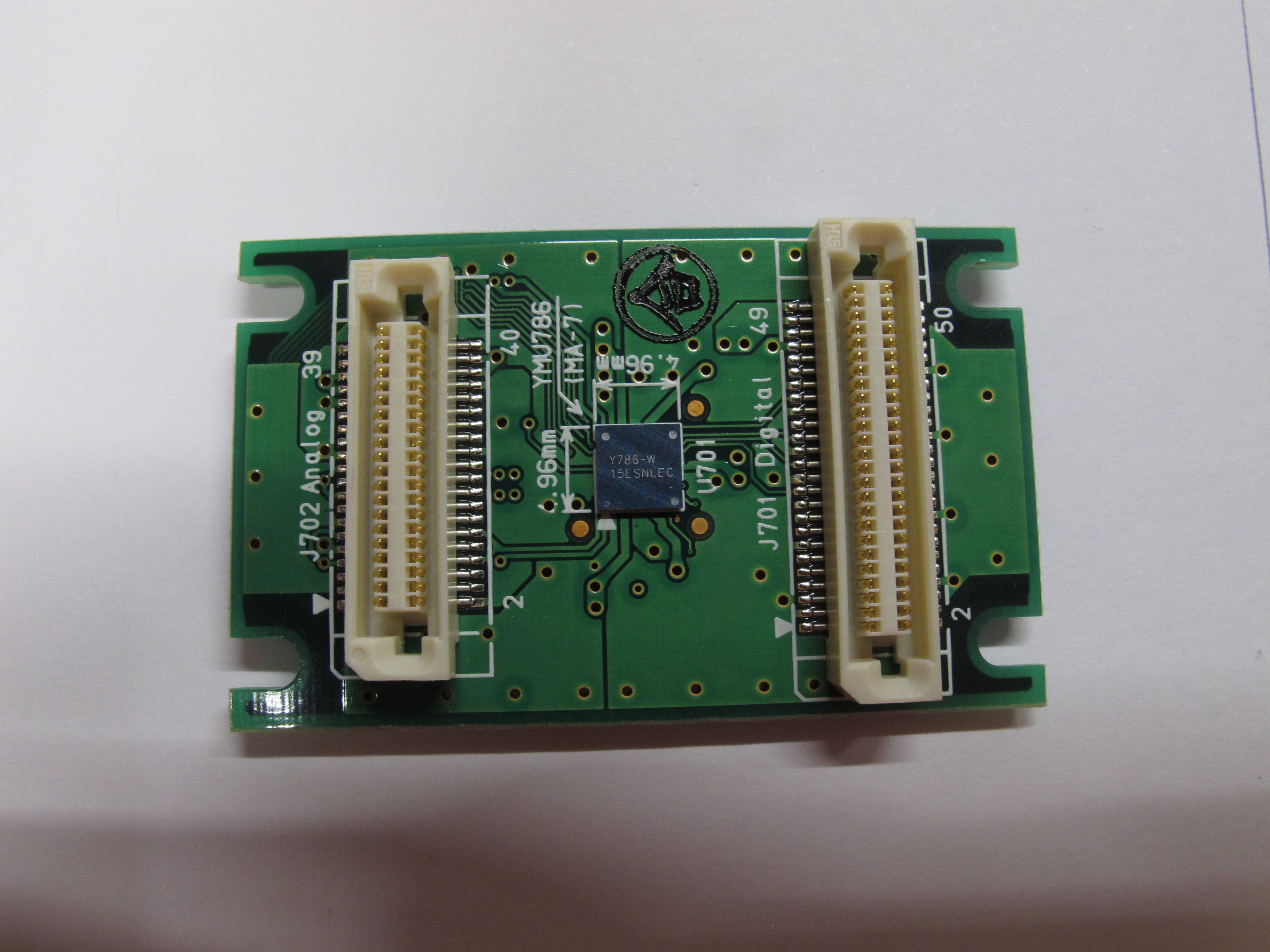
| The elevated PCB shows its belly. |
 |
|---|
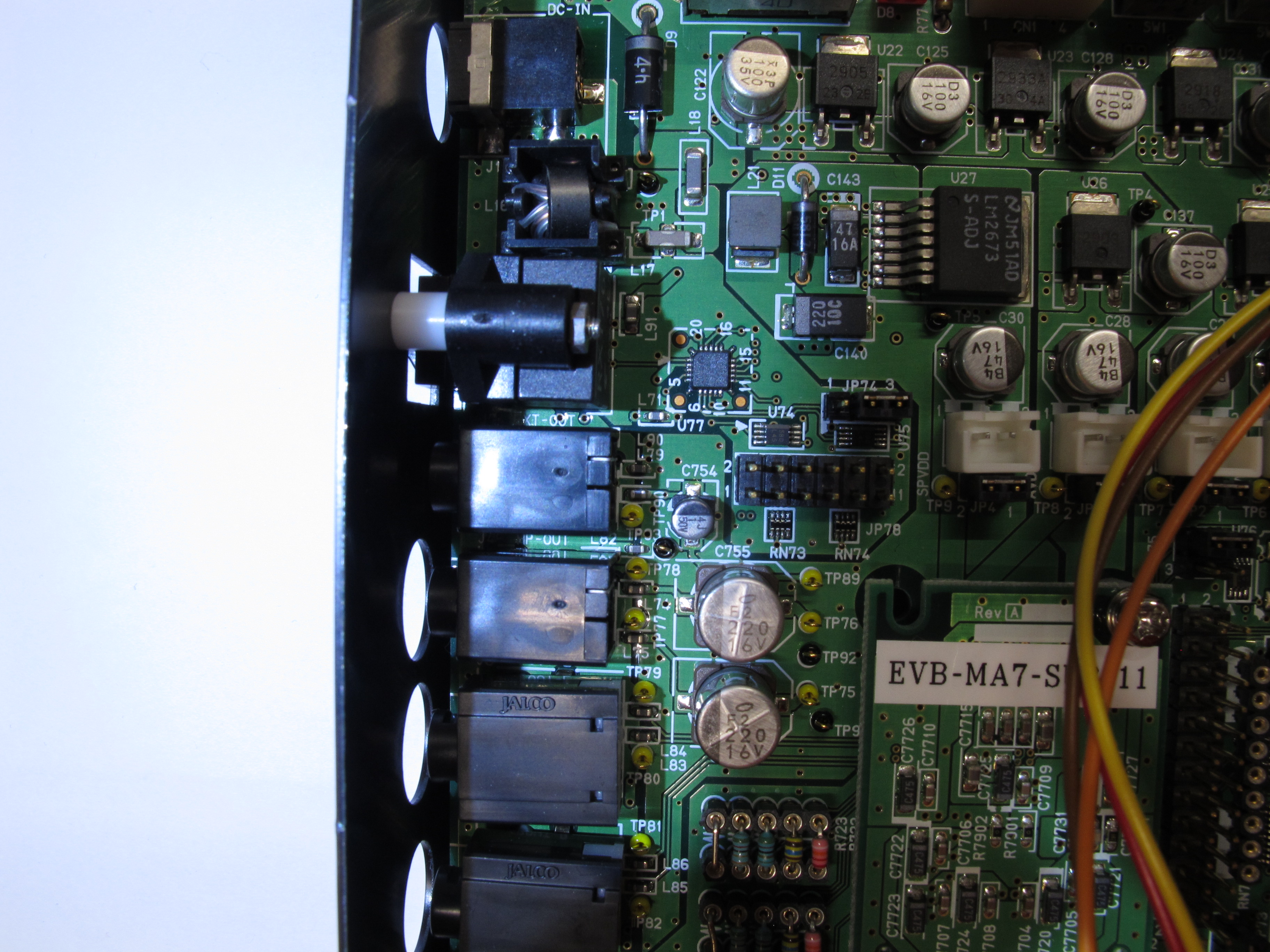
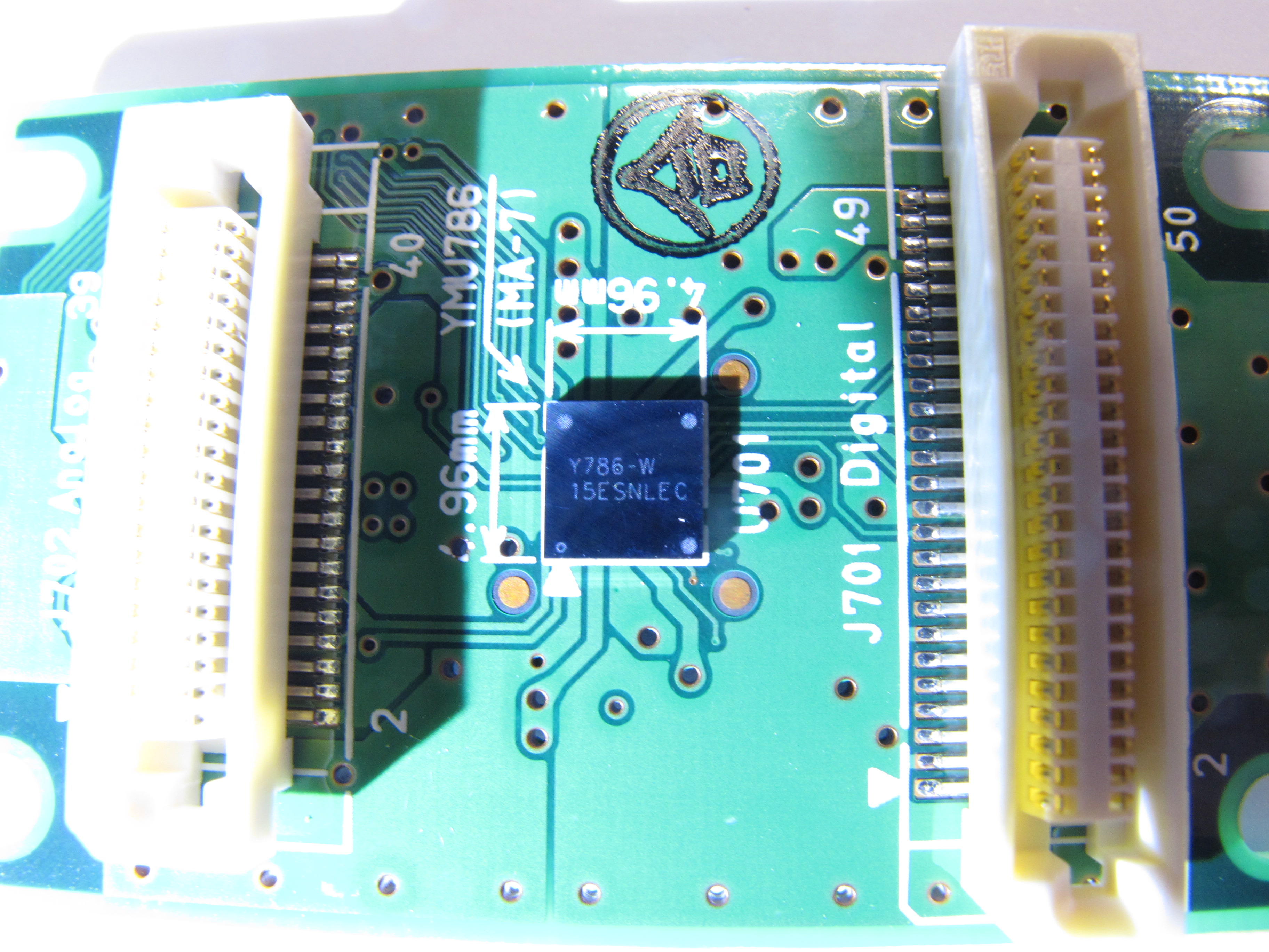
| For absolute idiots they wrote both commercial and internal names of the chip. |
 |
|---|
| Chip is in some ceramic BGA package. |
 |
|---|
| Tried to take a pic to later guess how many layers the PCB has... |
 |
|---|
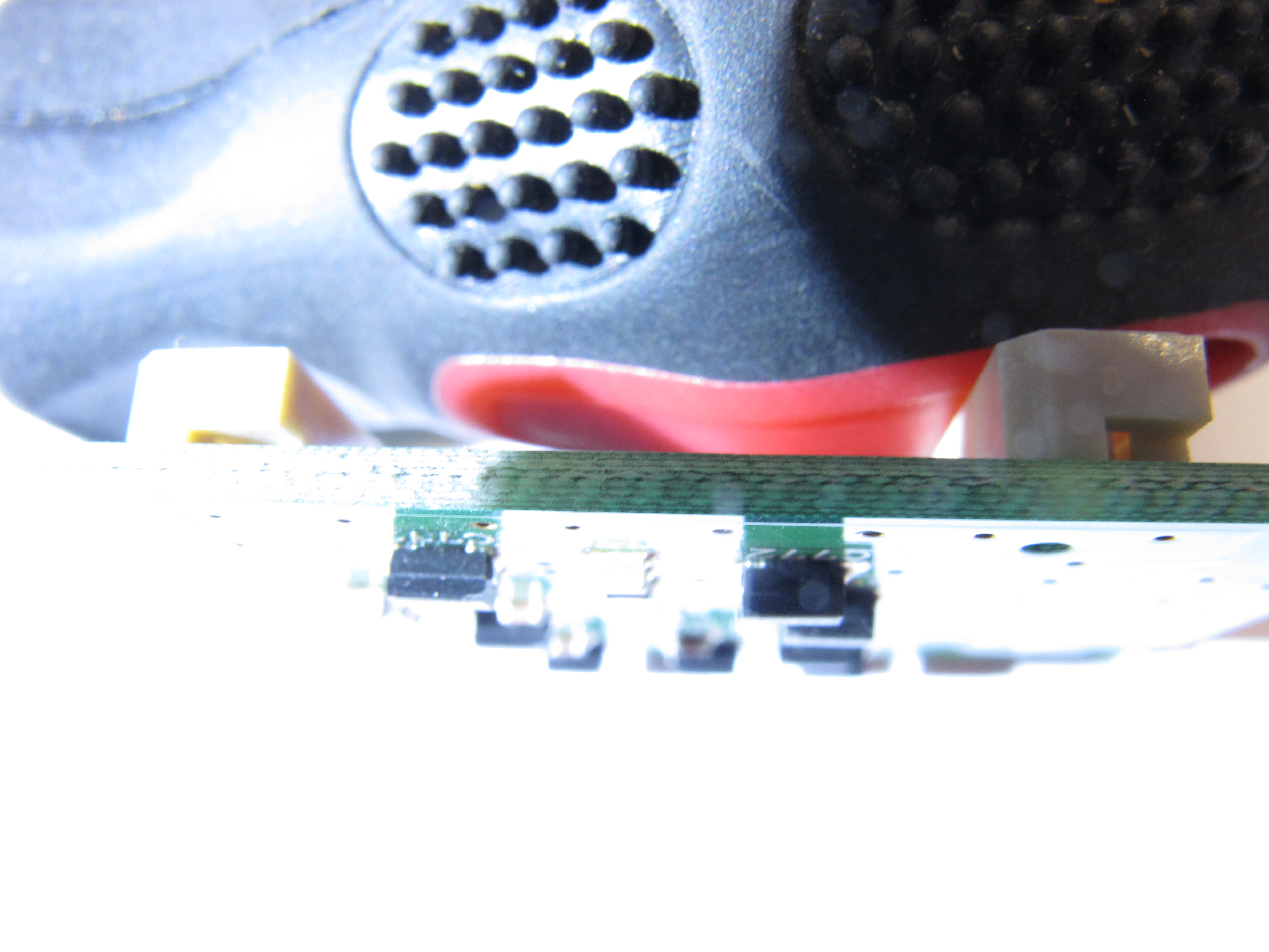
| And one more. This screwdriver handle will be featured in several future episodes too. |
 |
|---|
| Two chips with identical H and W dimesions may have different number of pins in BGA package. Here I tried to peek. |
 |
|---|
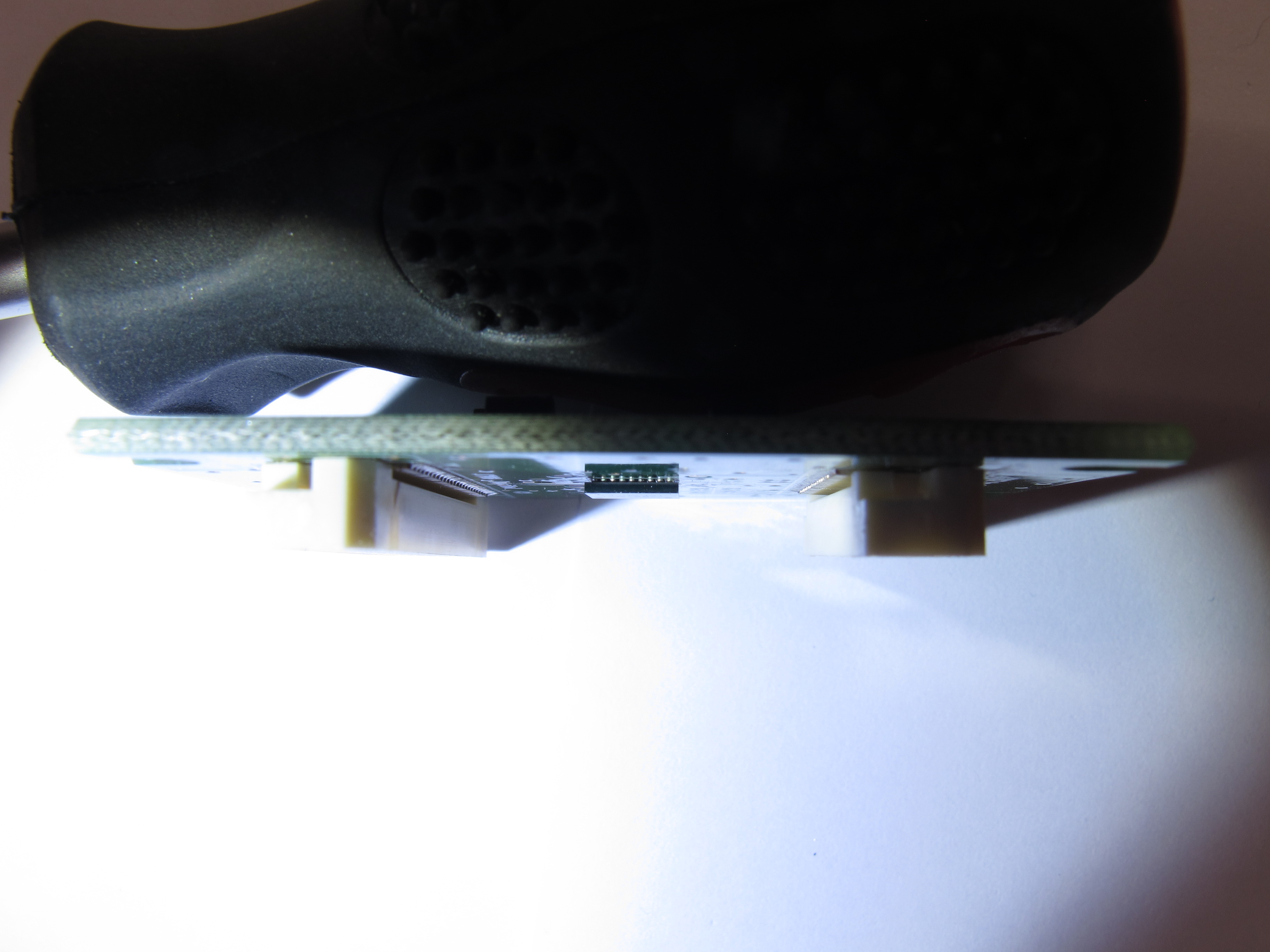
| Second attempt. |
 |
|---|
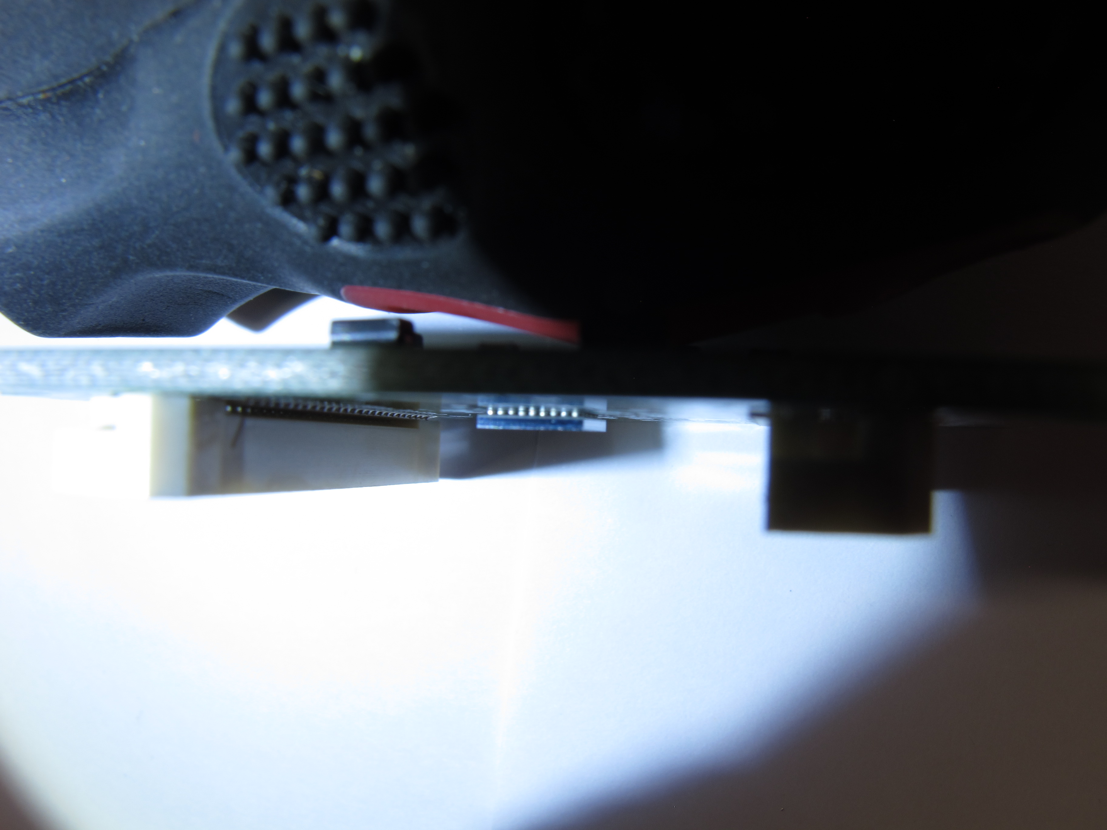
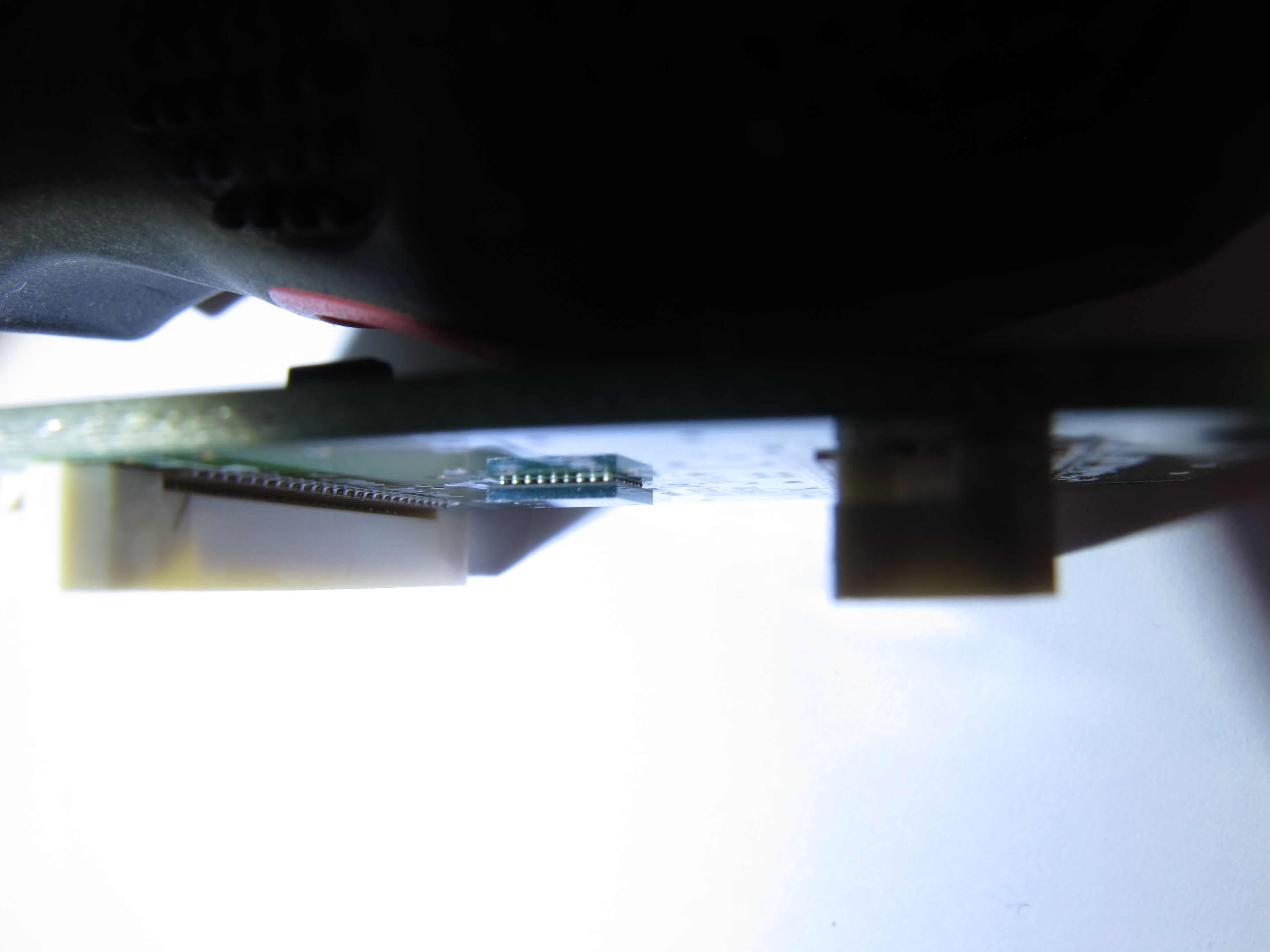
| Final attempt, hand tired. |
 |
|---|
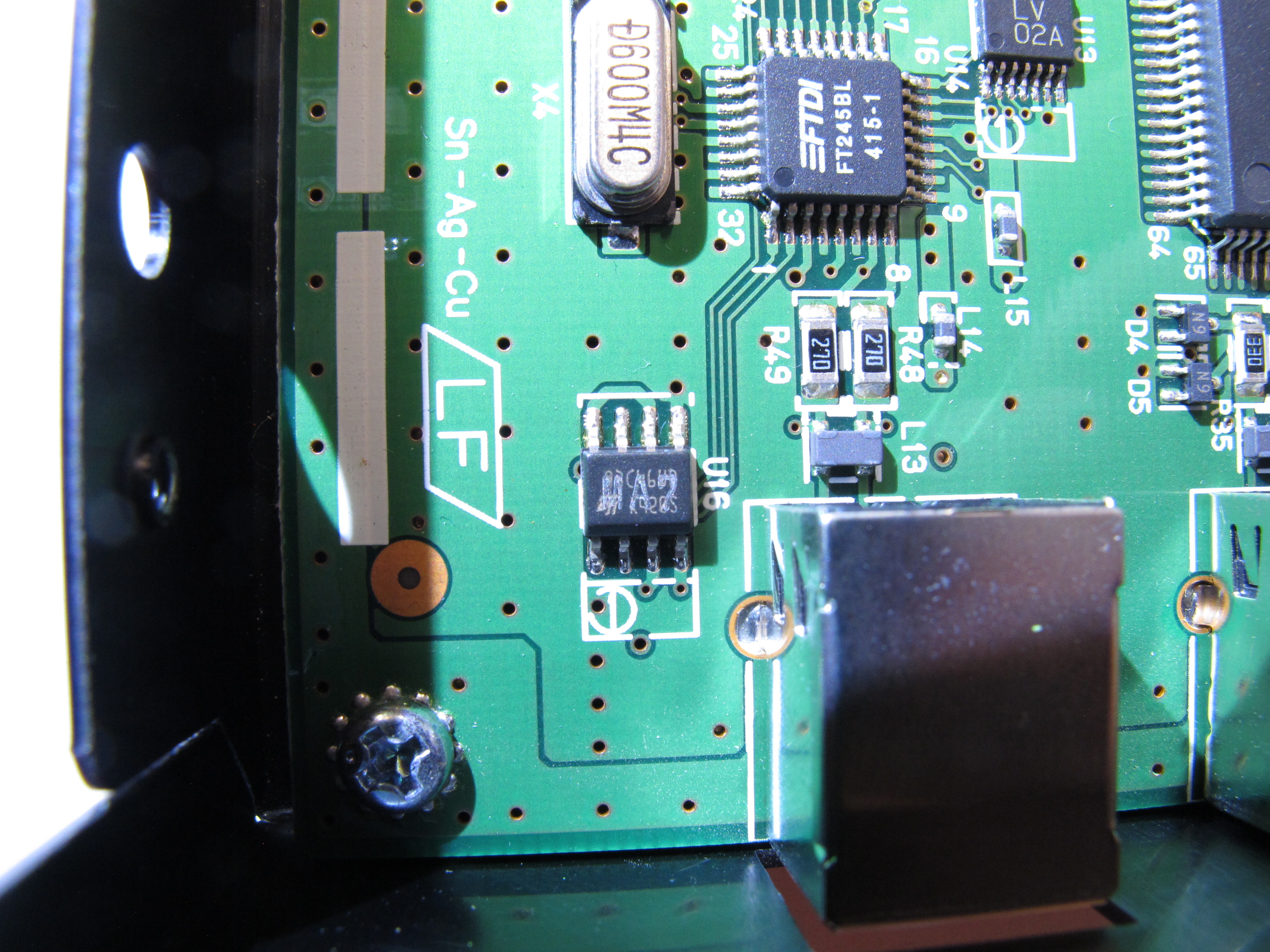
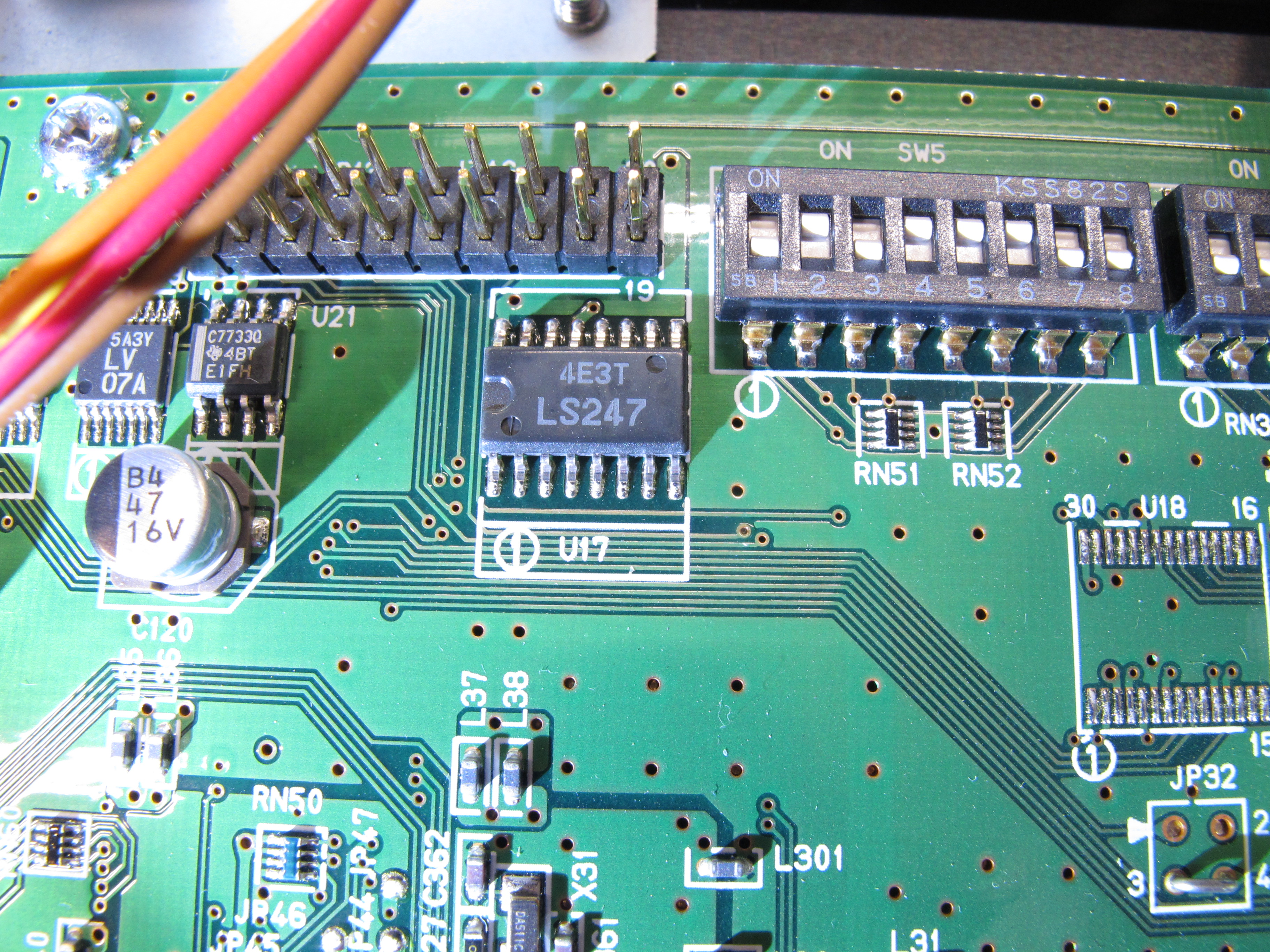
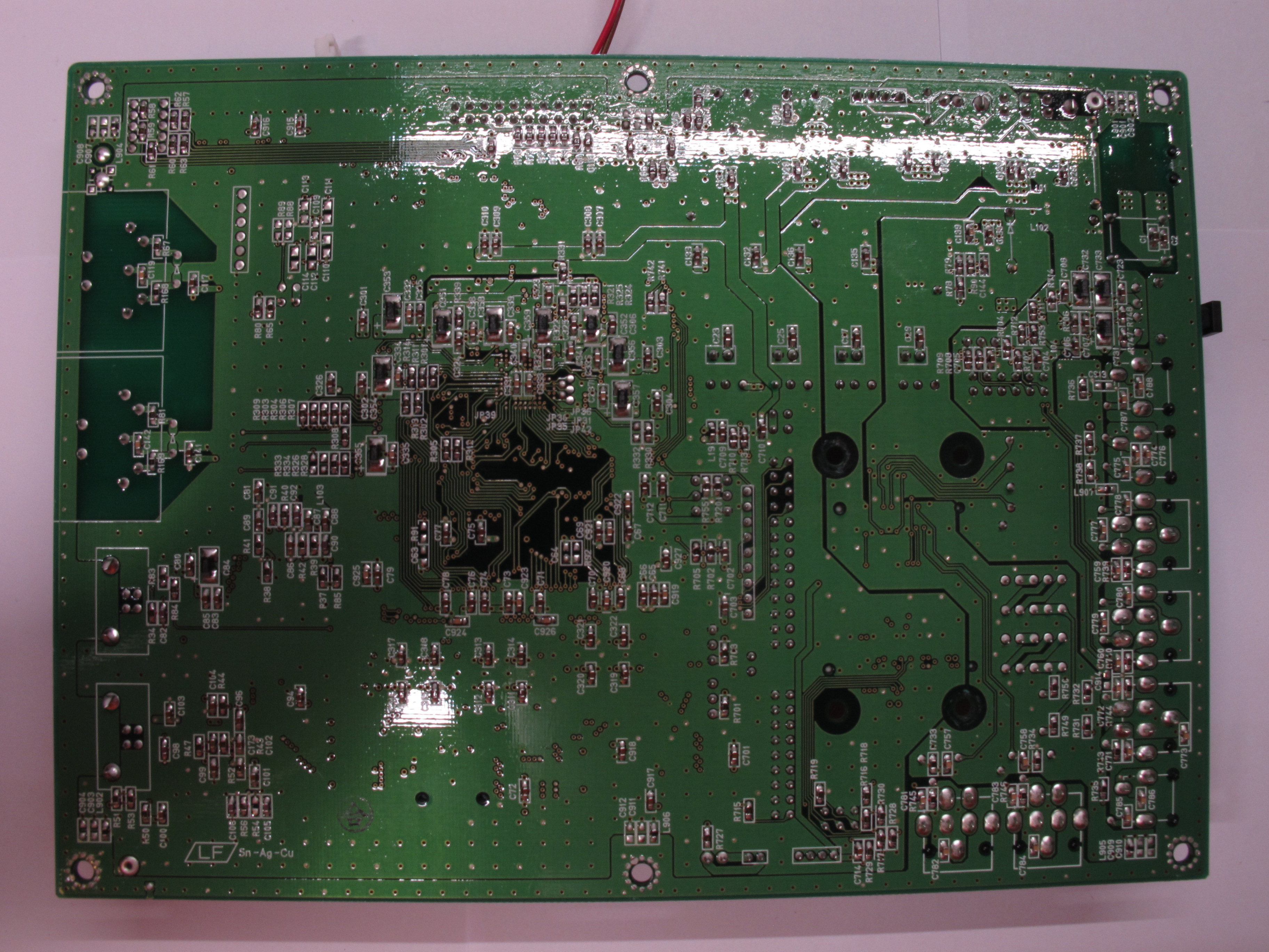
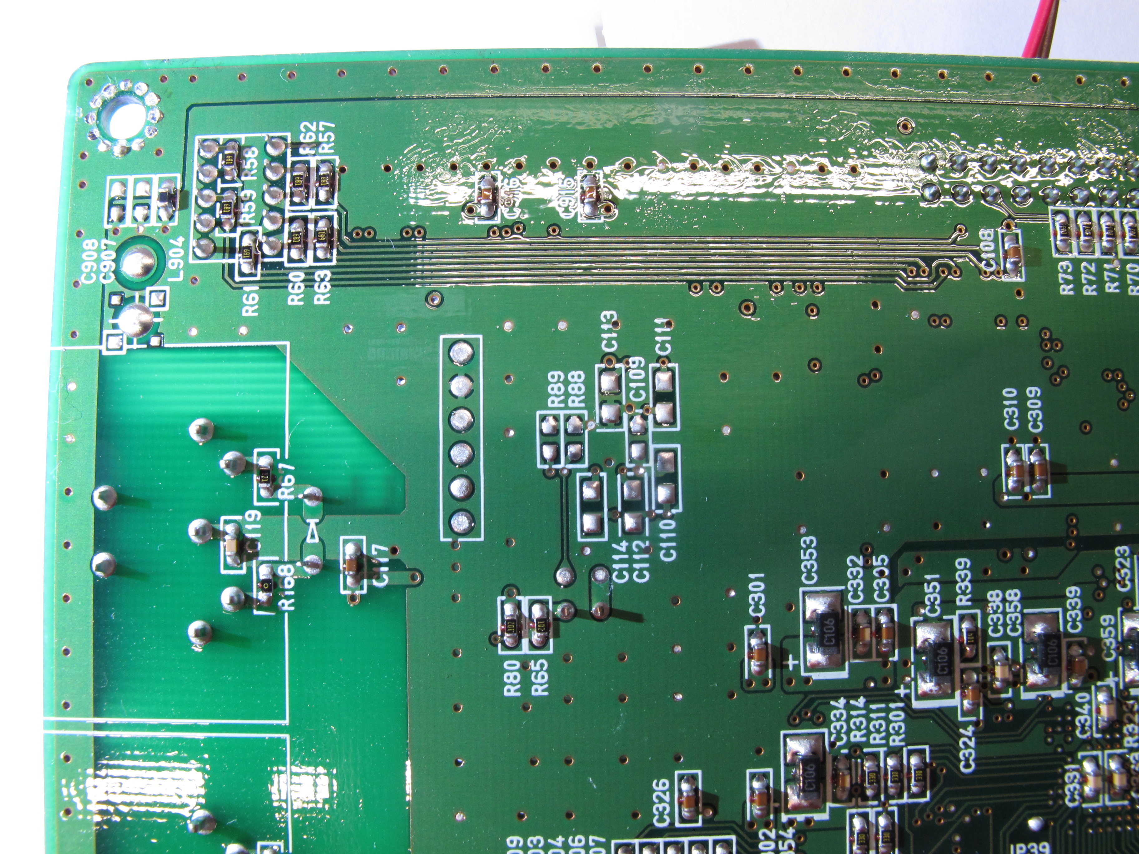
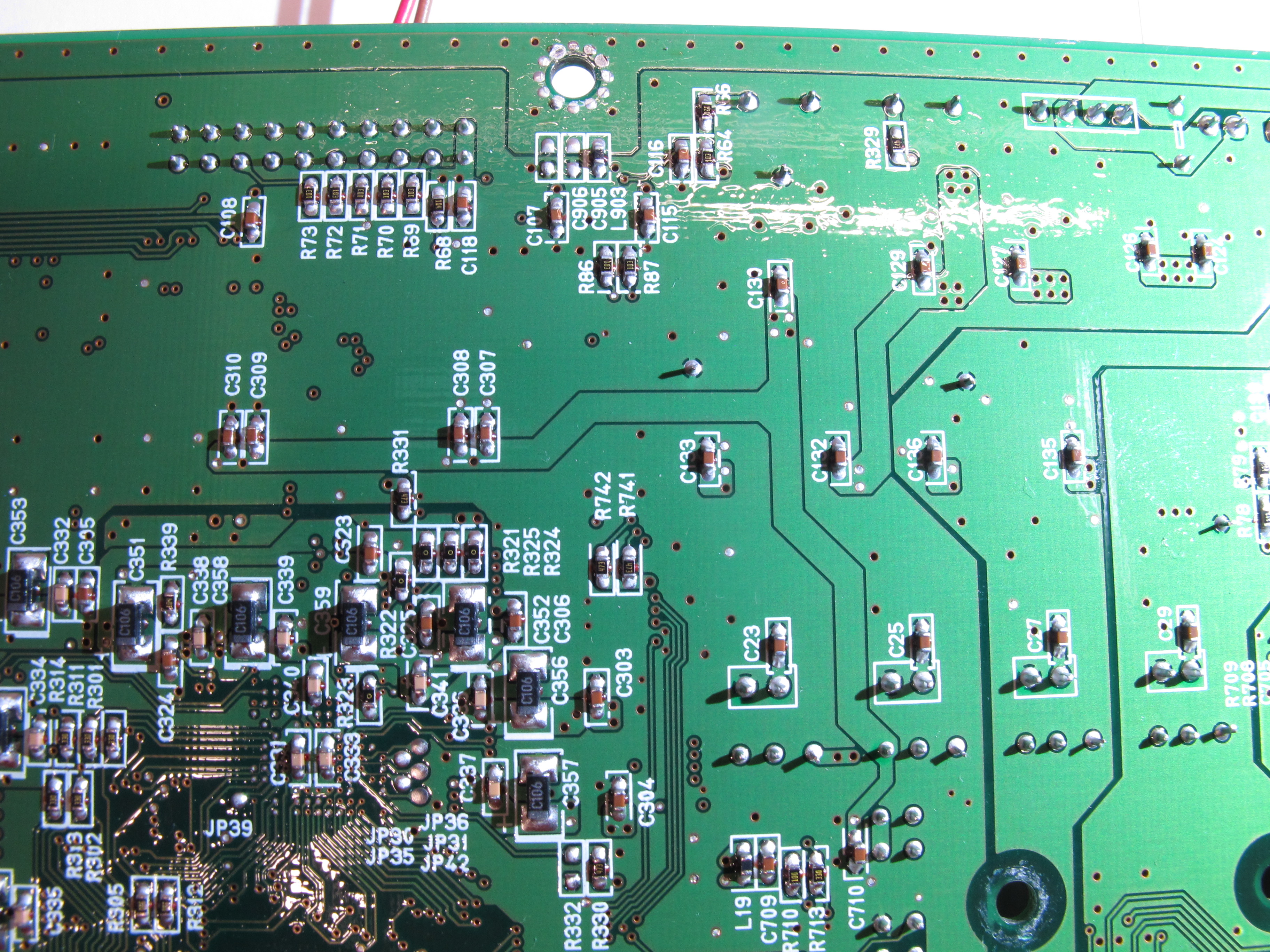
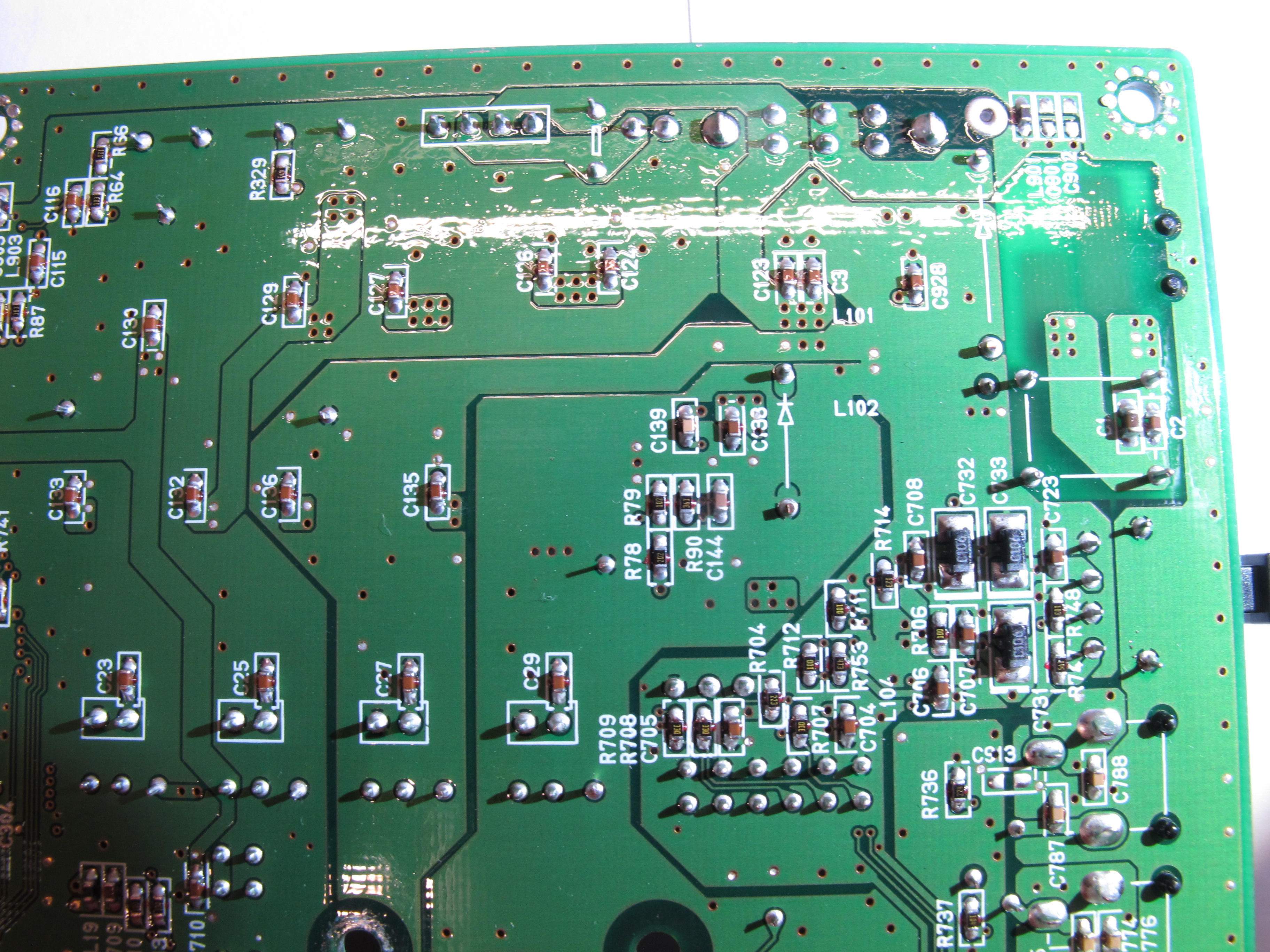
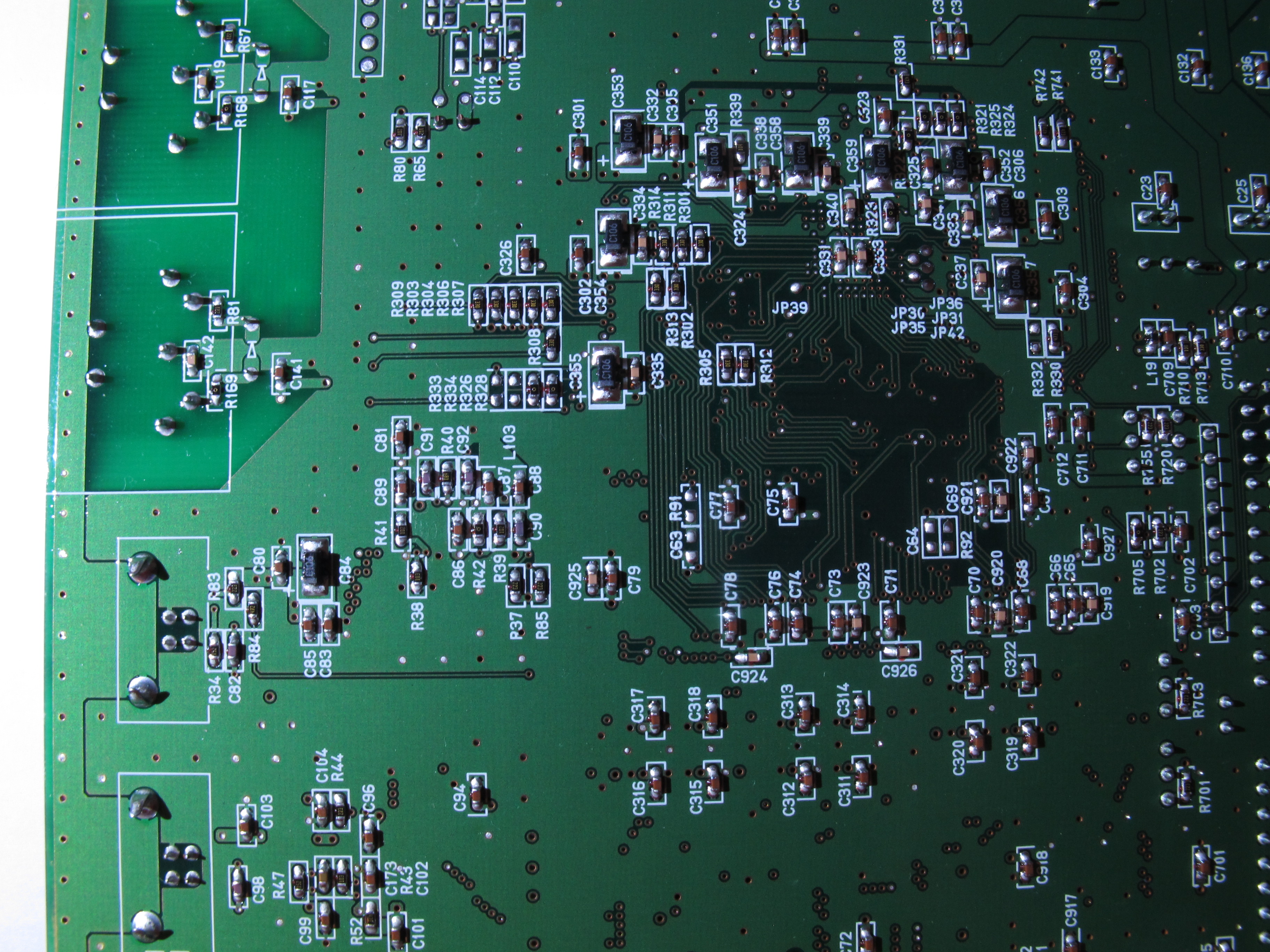
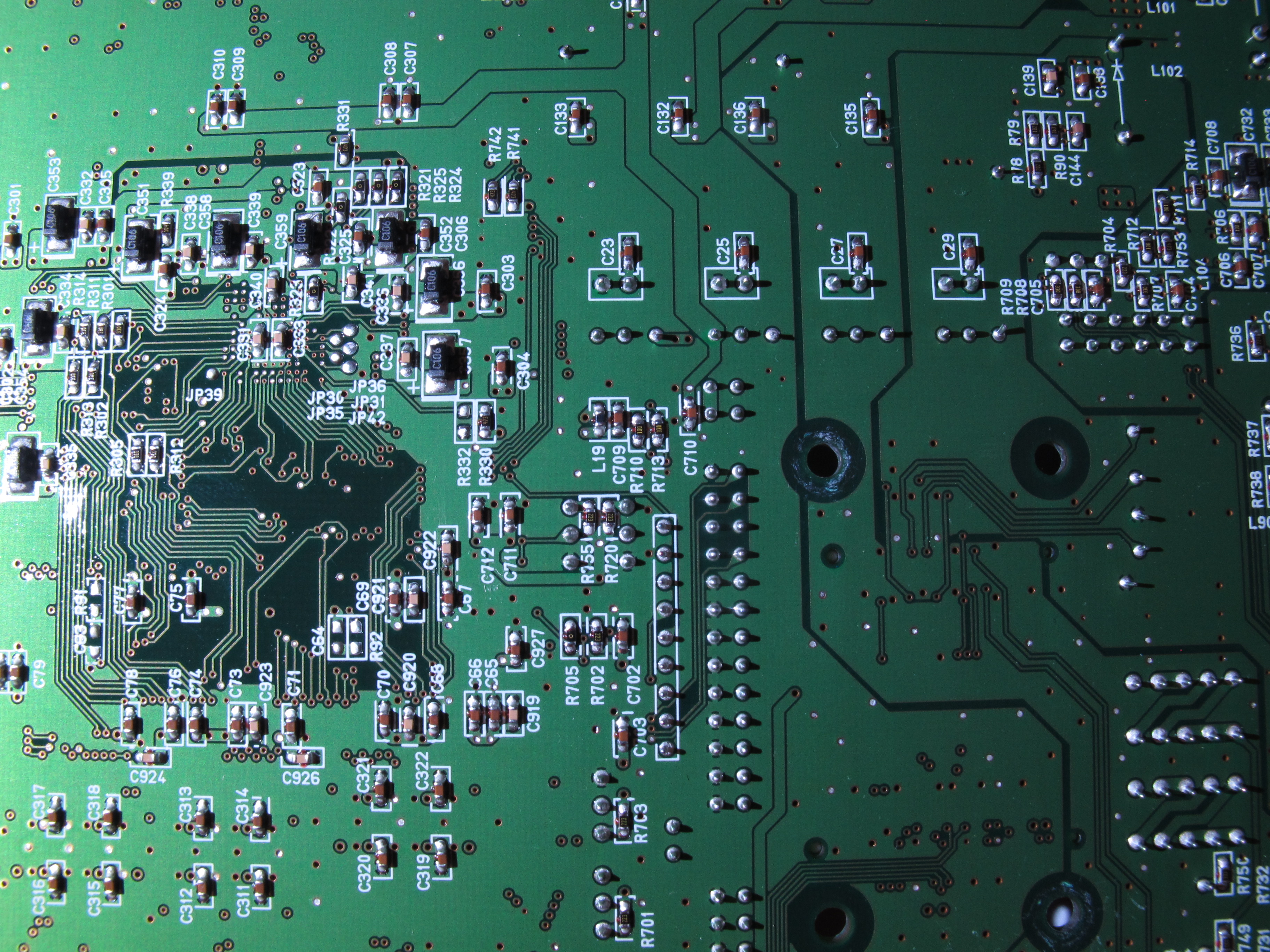
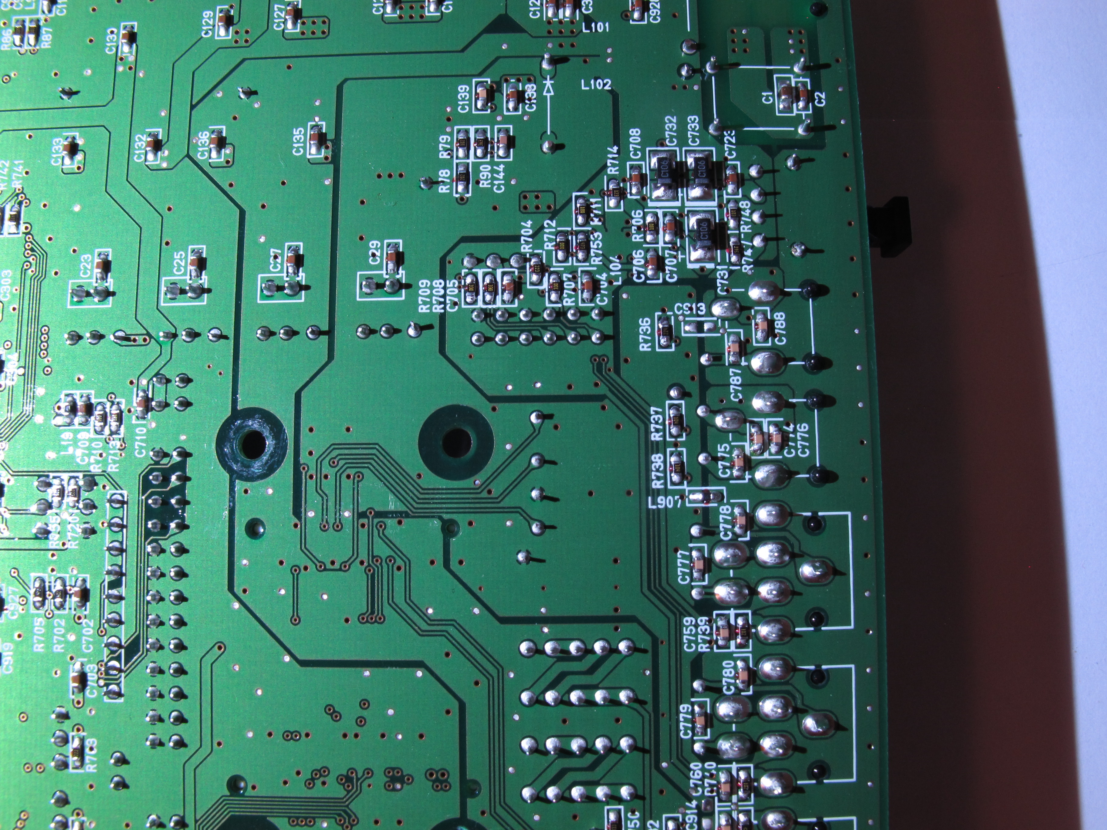
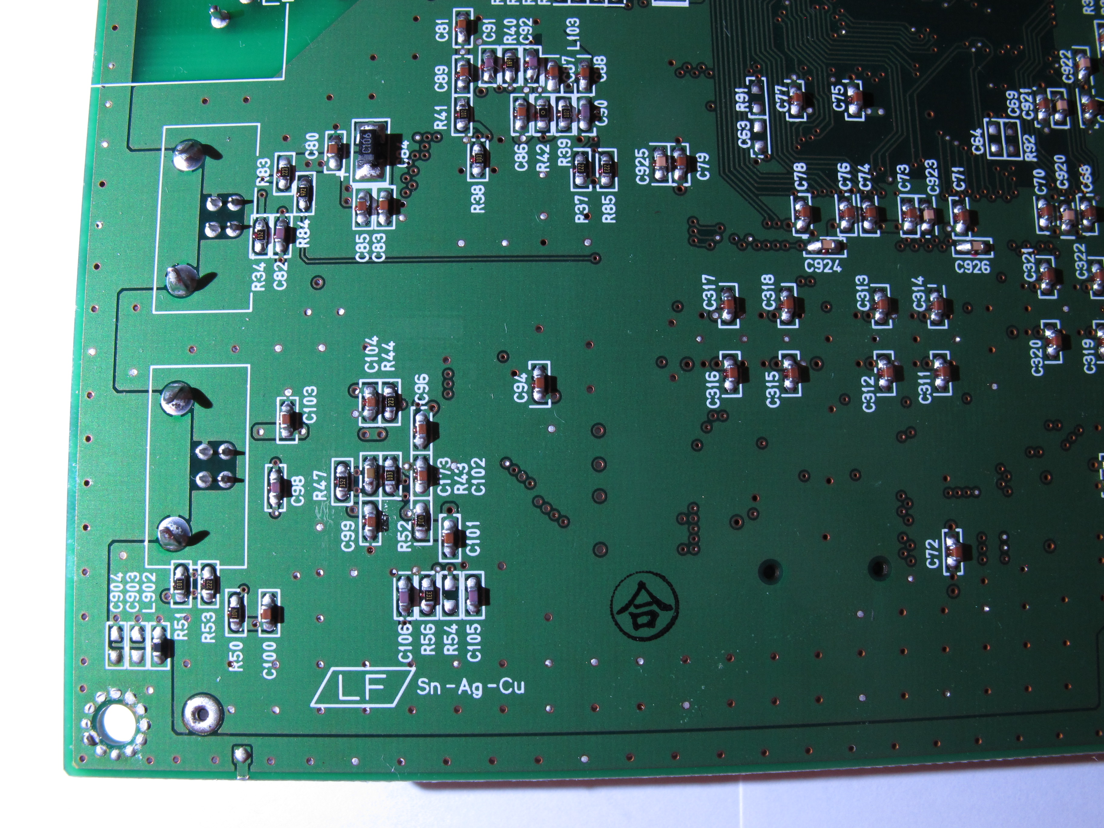
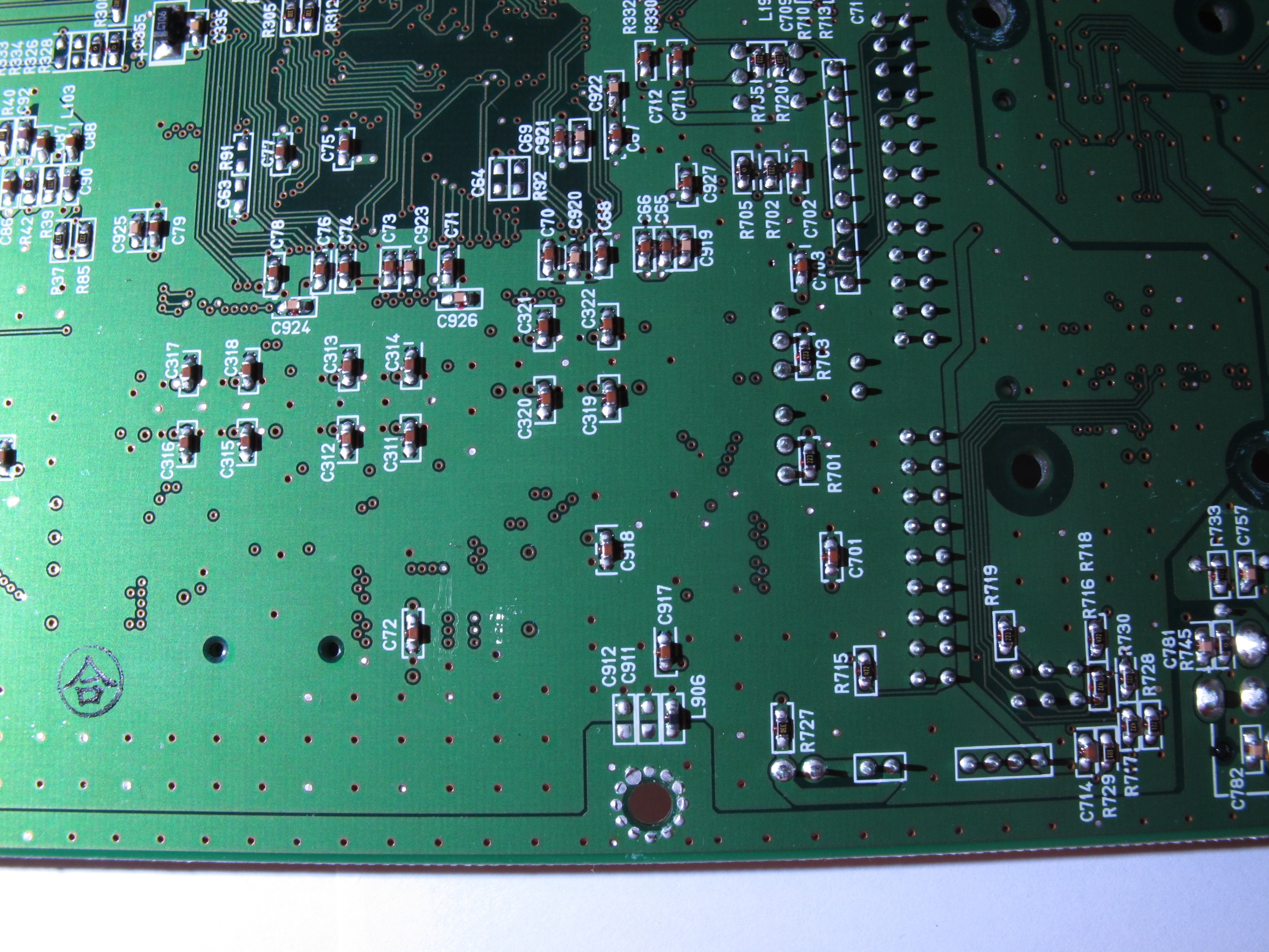
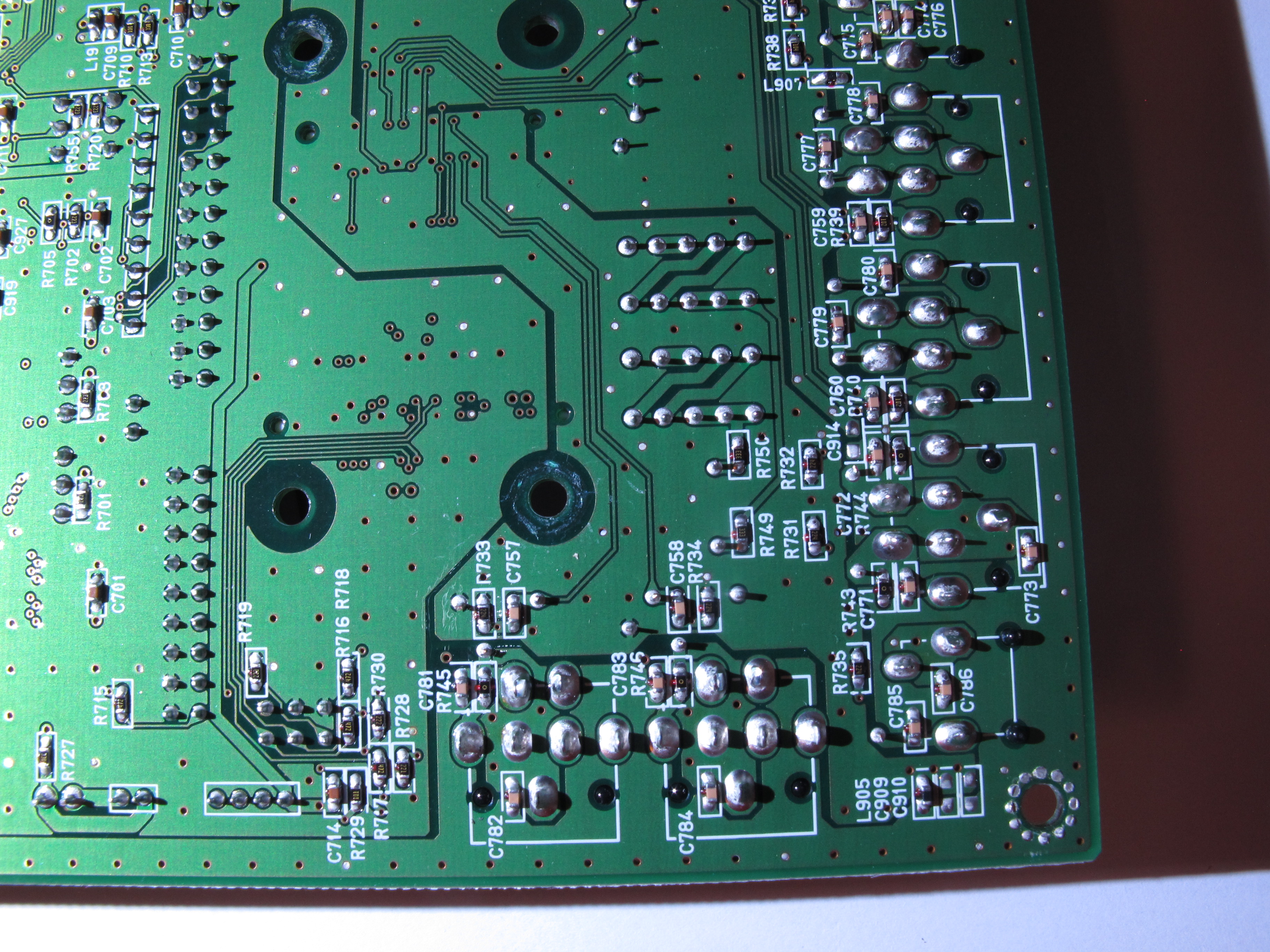
| Underside of main PCB. Below just shots of its sections, no comments |
 |
|---|
 |
|---|
 |
|---|
 |
|---|
 |
|---|
 |
|---|
 |
|---|
 |
|---|
 |
|---|
 |
|---|
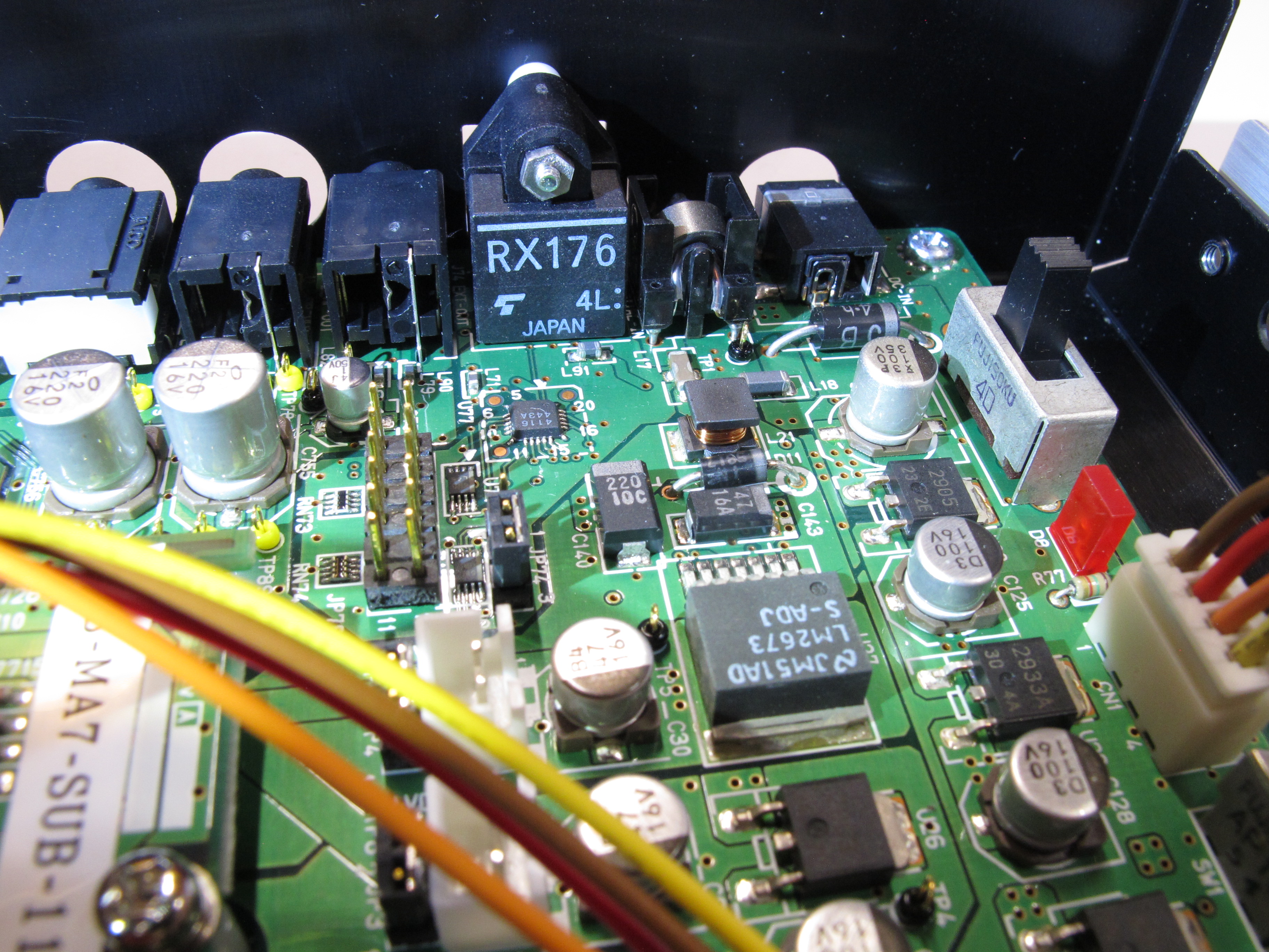
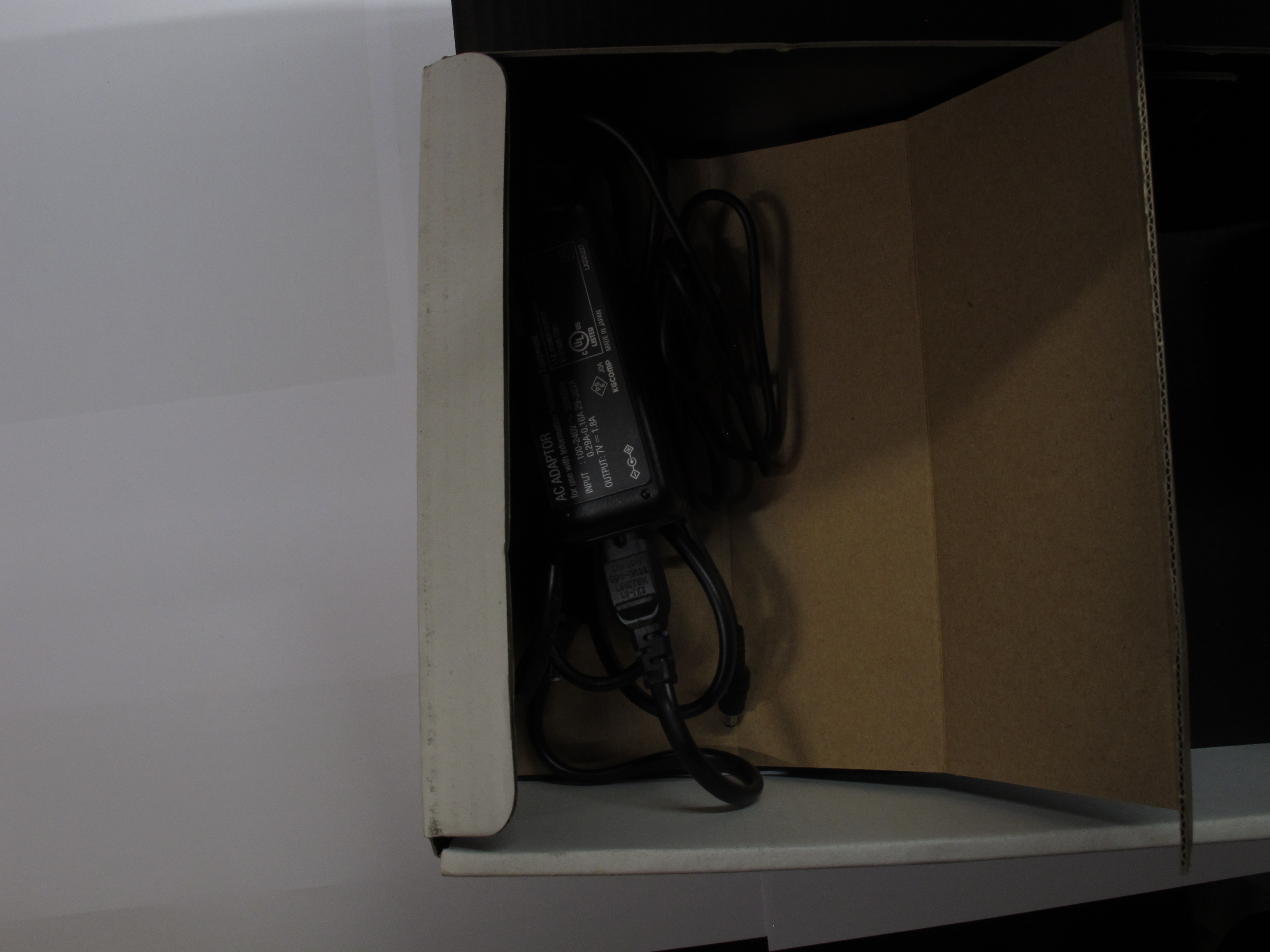
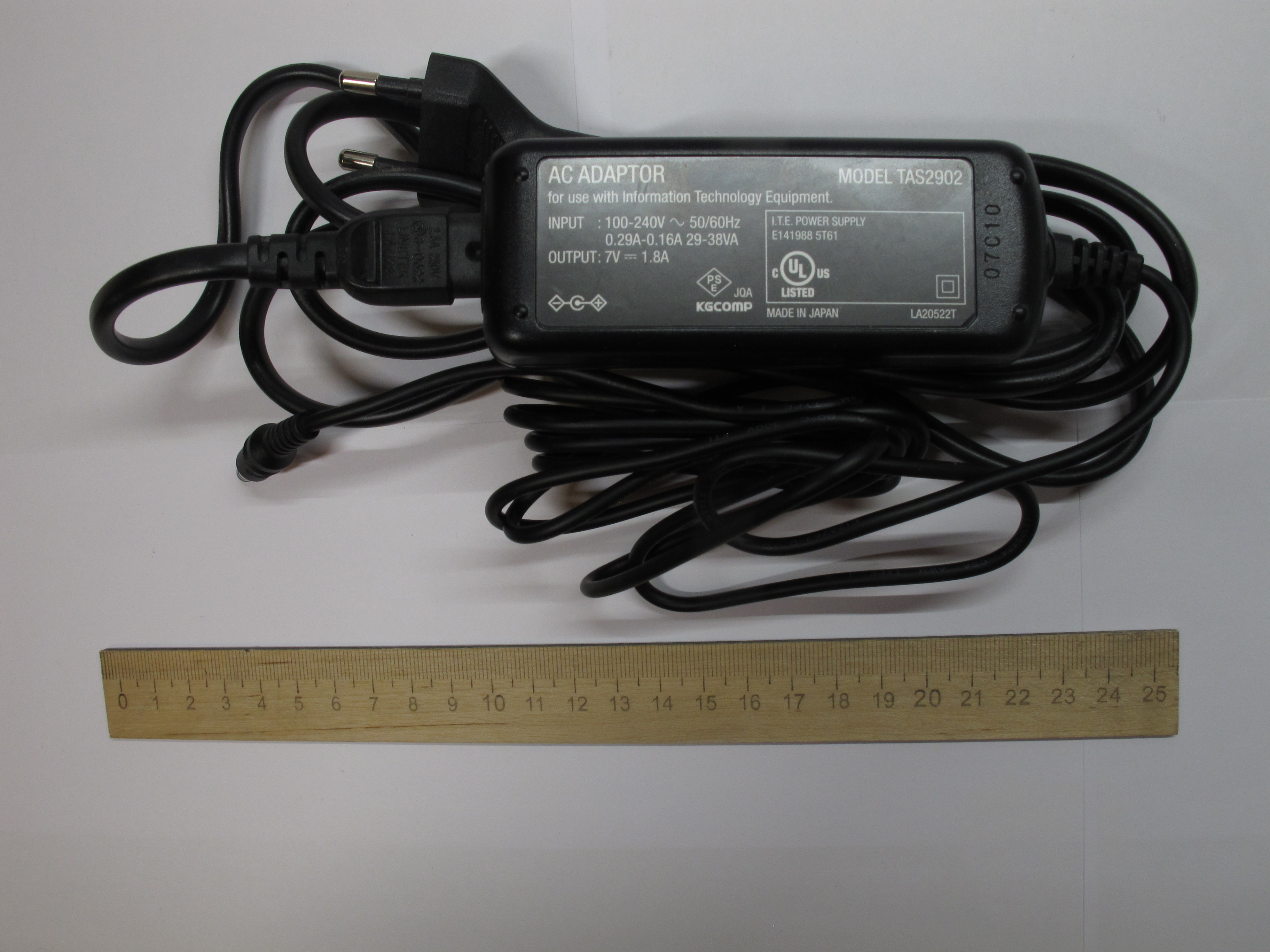
| Power supply. |
 |
|---|
| Alone. |
 |
|---|
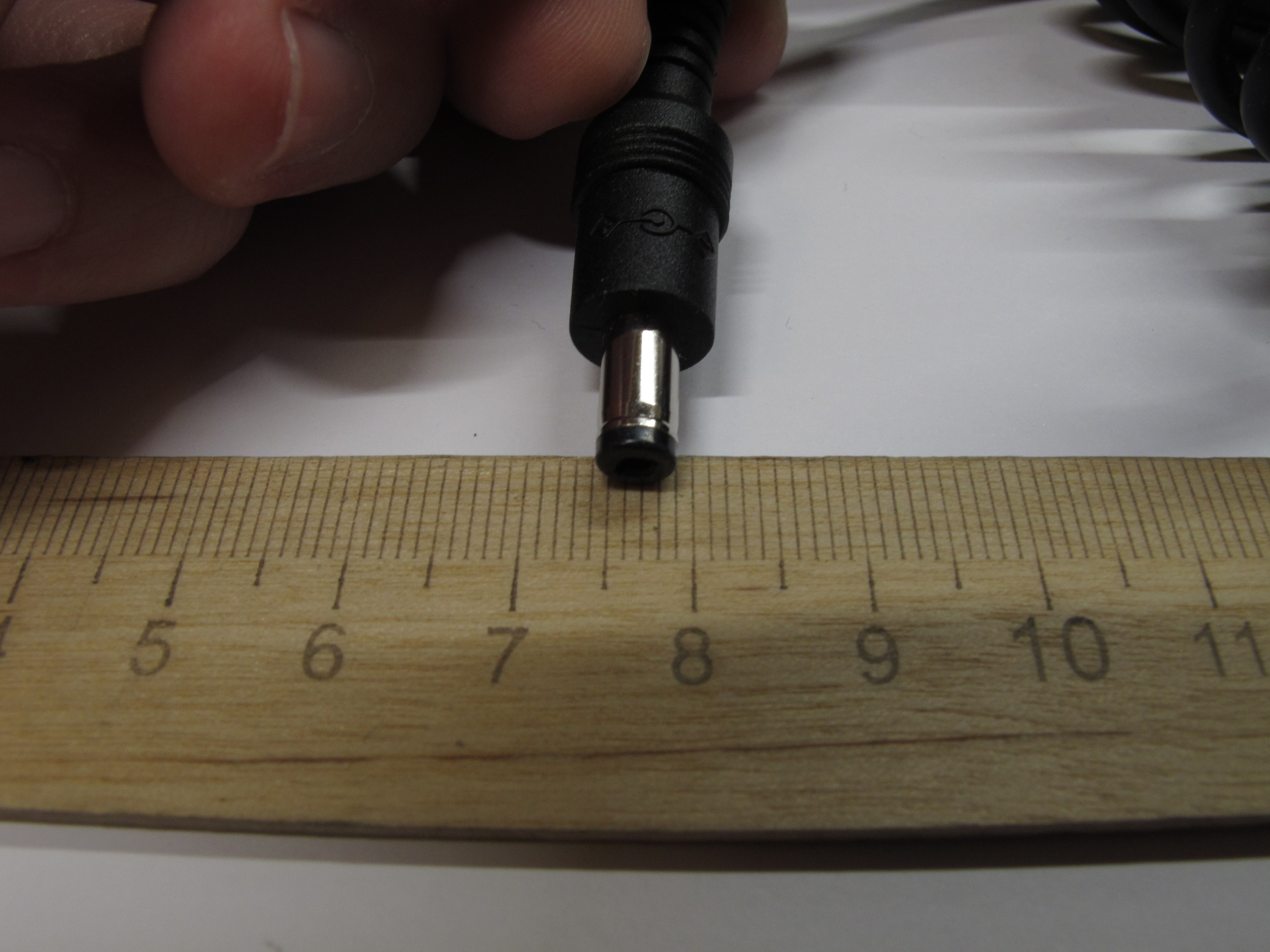
| Plug dimesions can be guessed. |